Managing Silkscreen Layers and PCB Stackup Information
Key Takeaways
-
The origins of the PCB silkscreen and what it is used for
-
Managing the silkscreen and other informational layers within the CAD database
-
How constraint management can help with the design of your PCB silkscreen

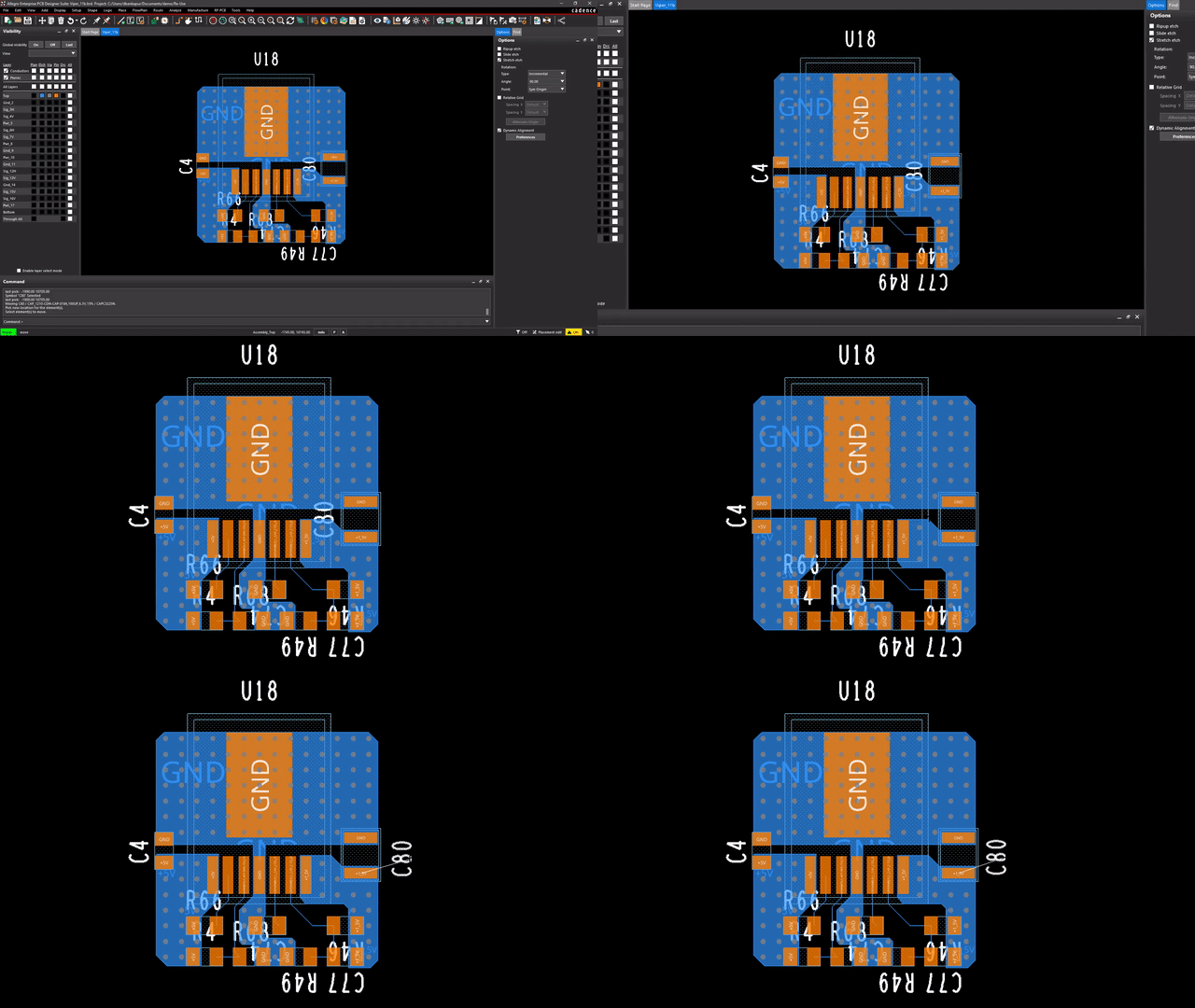
Adjusting silkscreen on your PCB - moving text to open space and changing the orientation for better readability.
Silkscreen printing with stencils is an art form that has been around for a long time. Stencils have been used throughout history to decorate the tombs of pharaohs and produce various religious images. Around the 15th century, silkscreen printing found its way to the West, where the original material used for the screen was silk. This resulted in it being given the name that it is known by today.
Today, most people are familiar with silkscreen printing being used to create their favorite images and patterns on T-shirts. What is less known is that a variation of this process has been used for years to create images and markings on printed circuit boards. How the images are rendered on the circuit board depends on the method used by the PCB designer in managing silkscreen layers and PCB stackup information in their CAD system. Let’s take a closer look at the PCB silkscreen process and some recommendations for silkscreen design best practices.

PCB Silkscreen: What It Is and What It’s Used For
Silkscreen is not only a type of printing process used to apply identification markings on a printed circuit board, but it is also the generic term used to describe the ink markings themselves. This is why the CAD tool layers devoted to these markings are referred to as the silkscreen layers. Printing the silkscreen onto the board is one of the last steps to be completed during printed circuit board fabrication. And while it is true that a manual silkscreen process is still used to create markings on a PCB, there are two other processes available as well. Below you’ll find all the silkscreen processes available and why you may or may not want to use them:
-
Manual silkscreen printing: This is the standard method of printing markings on a PCB by using a stencil as a template and pushing a non-conductive ink through a polyester screen onto the board. The limitation in this process is the width of the ink which can’t get any smaller than 0.007 inches.
-
Liquid photo imaging (LPI): For ink images that are smaller in size and require greater accuracy, the LPI process will be used instead. Just like the application of solder mask to a circuit board, a liquid photo-imageable epoxy is applied, exposed under UV light, and then developed and cured.
-
Direct legend printing: This is the most accurate method of printing silkscreen markings on a circuit board, but it is also the most expensive. Acrylic ink is applied using an inkjet printer working directly from the data in the CAD design manufacturing files.
The silkscreen’s primary purpose is to mark the position of the components on the board with an outline, and the part’s unique reference designator. Silkscreen is also used for component polarity and pin 1 indicators. As the component density on printed circuit boards continues to increase, however, there is less space for silkscreen information to be printed. It is common therefore to see reference designators abbreviated as a sequence of numbers, and often the outlines themselves are completely omitted. This doesn’t lessen the need for component identification though, as these are still important for prototype, NPI, and limited-run boards that will require manual assembly. Component identification is also important for boards that are assembled using automated systems for test and debug purposes, as well as automated optical inspection (AOI), and manual inspection.
Silkscreen markings are also used for marking non-component information as well. This can include the name, part number, and revision of the circuit board, as well as corporate contact information, copyrights, and manufacturing markings. The silkscreen conveys a lot of information about the circuit board, but it isn’t the only method of communicating board information. PCB design CAD systems have many layers built into them that can be used for board information other than the silkscreen, and we will take a look at that next.
Working with the component outlines and reference designators on the silkscreen layer in a PCB design
Additional PCB Information Layers
While the PCB silkscreen is intended to identify the component locations and reference designators, it rarely is able to completely do this. This is especially noticeable on circuit boards with a lot of components, which can end up covering a lot of the silkscreen markings. Another problem is that silkscreen ink is generally not desired to go into holes drilled for components and vias. The post-processing routines in the PCB design CAD systems will usually remove the ink that is going through these holes. On densely routed boards with a lot of vias, this can result in the silkscreen layer having the majority of the component outlines removed. For this reason, the same component information that is on the silkscreen is duplicated on another CAD system layer dedicated to the manufacturing assembly drawing.
The assembly drawing usually shows an enlarged view of the board with the component outlines and reference designators clearly labeled without any conflicting holes or routing. Paper copies of these drawings used to be used on the production floor to assist in the PCB assembly, but now these drawings are transferred electronically in PDF or other drawing formatted files. While the manufacturing of a circuit board is being driven more and more by CAD data instead of drawings, most manufacturers still want to see an assembly drawing to verify the production of the board. There is a lot of different information that may be required in the manufacturing of the circuit boards, which can be organized and presented on different layers in the CAD system. Here are some examples of some of the information layers that can be included in a circuit board’s layer stackup:
-
Silkscreen layers
-
Assembly drawings
-
Component outlines
-
Component dimensions
-
Component footprint and/or part numbers
-
Testpoint maps
The silkscreen and the rest of these informational layers need to be managed within the PCB design tools, and we will look more into that in the next section.
The Cross-Section Editor in a PCB Design CAD tool showing the different layers including the silkscreen
Managing Silkscreen Layers and PCB Stackup Information With PCB Design CAD Tools
A circuit board is made up of a combination of the following layers and materials to build the physical board stackup:
-
Trace routing
-
Power and ground planes
-
Dielectric material
In addition, the following materials will be added onto the board to complete the fabrication of the board and prepare it for component assembly:
-
Solder mask
-
Solder paste
-
Silkscreen
To accurately provide the required manufacturing data, the PCB design tools will have a representation for these layers and materials within its database. In addition to these electrical and non-electrical layers, there will also be the layers we listed earlier for informational purposes such as assembly drawings. To control all of the different layers in a PCB design CAD system, a layer stackup management system like what is shown in the picture above is usually used.
There are also many other controls in place inside a PCB design CAD system for working with silkscreen and the other board and informational layers. One example is how the systems will give you the ability to turn on and off the display of these layers, as well as to change their colors and fill patterns. In some of the more advanced CAD systems, you will have control over the different elements on a layer. In Cadence Allegro, for instance, you can change the color and display of the silkscreen reference designators separately from the component outlines on the same layer.
PCB design CAD systems give their users a lot of control over how the data is displayed and used. They can also help their users with the design of silkscreen layers to avoid some of the more common manufacturing problems that can occur during manufacturing.
Checking silkscreen clearances in Cadence Allegro’s PCB Editor
Using the DFM Checking in PCB Layout Tools to Verify Silkscreen
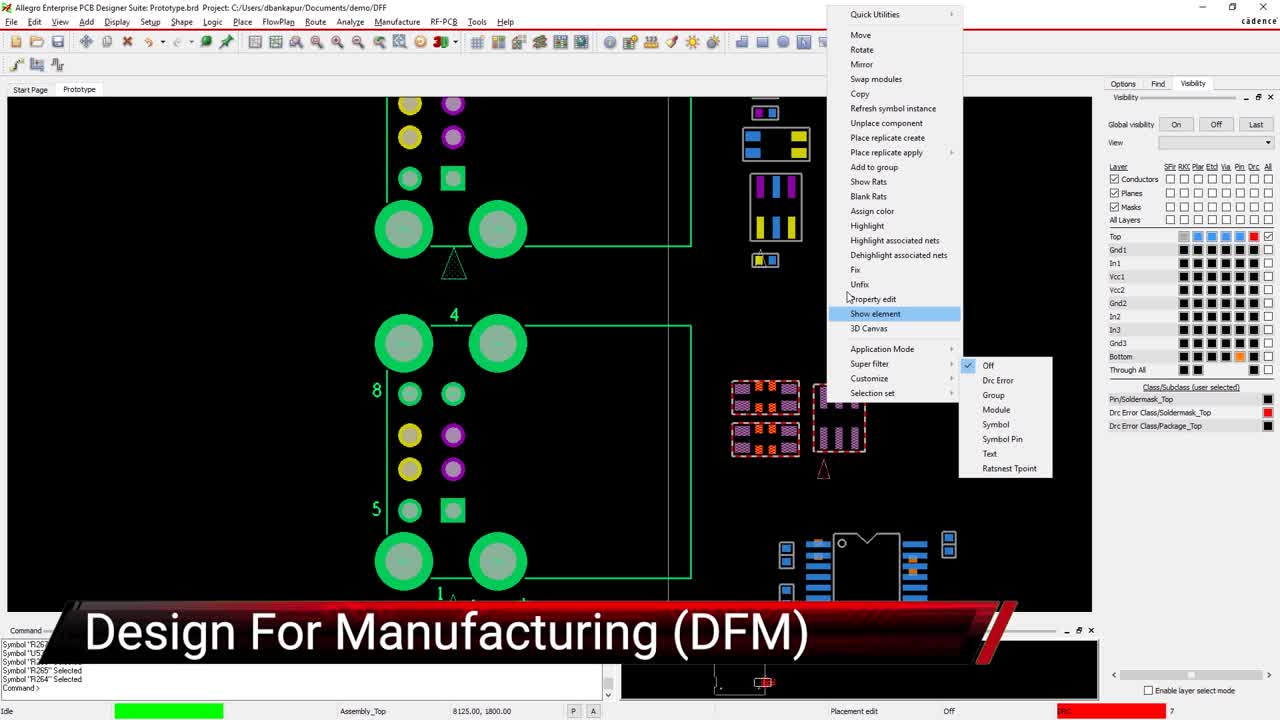
Advanced PCB design CAD tools, like the Allegro PCB Editor, give you a lot more functionality than just placing components and routing their nets together. These tools will also give you the ability to check the design against a set of rules and constraints that you have control over. For example, the constraint manager in Allegro will allow the designer to set up multiple rules and constraints for designing their circuit boards. These not only guard against creating electrical shorts and other errors, but they also help guide the design of high-speed nets to ensure their maximum performance. The constraint manager can also help with the design of the circuit board’s silkscreen.
Part of Allegro’s constraint manager is the ability to set up specific rules for manufacturing. These rules are further separated into design for assembly and design for fabrication rules, and within the fabrication ruleset is the ability to configure silkscreen clearance rules as shown in the picture above. These rules will help guard against getting silkscreen too close to component pads or holes in the board that could cause a problem for PCB fabrication. It will also ensure that you don’t use silkscreen line widths and font sizes that are too small for the printing processes being used.
To find out more about PCB design and how to lay out a circuit board, take a look at this E-book.
If you’re looking to learn more about how Cadence has the solution for you, talk to us and our team of experts.