What is Thermal Design in HDI? Managing Heat in Ultra-Thin Dielectrics and Microvia-Dense Regions
Thermal design in high-density interconnect (HDI) is the set of strategies engineers use to move heat away from hot components in densely packed printed circuit boards (PCBs). As electronics shrink, more power dissipation gets concentrated into smaller areas. The mental model that matters most for HDI thermal work is this: copper structures provide most of the heat spreading due to their high thermal conductivity, while dielectric layers provide the through-thickness thermal path between copper regions with significantly higher thermal resistance . And a surprising finding about thermal vias that go against the typical assumptions involved in using them for heat dissipation. This post covers how that model plays out in real designs, which structures contribute most to cooling the PCB, the proper use of thermal via arrays, and finally, copper balancing strategies that prevent warpage during fabrication.
Designing Effective Thermal Via Arrays
Thermal vias connect a hot component pad to a copper plane on another layer. The vias are the bridge. The plane is what spreads and sinks the heat. Both matter, but the plane does most of the cooling work.
Brooks and Adam tested this with thermal simulation. In their setup, a hot pad with no plane underneath ran at about 82°C, which is 62°C above ambient. Adding a small plane on the opposite side with one thermal via brought it down to about 79°C, only a 3°C drop. Replacing the small plane with a large copper plane (no thermal vias at all) brought the pad down to about 43°C, roughly 23°C above ambient. The large plane alone did most of the cooling. Adding five thermal vias on top of that large plane shaved off only a few more degrees.
The design takeaway: plan the plane first, then the vias. A robust ground or power plane on the layer below your hot component does the heavy lifting. Thermal vias get heat from the surface pad to that plane.
In HDI designs, via geometry matters because microvias have less cross-sectional area than plated through-vias. A plated through-via at 12-mil finished diameter with 1-mil plating has a copper ring of about 34.5 square mils. A filled 4-mil microvia has a solid copper area of about 12.6 square mils, roughly one-third the area.
Because microvias contain less copper cross-sectional area than larger plated through-vias, higher microvia counts are often required to achieve similar vertical thermal conductance. The benefit of microvias is they pack densely, so the extra count fits in tight regions.
For high-power components, a hybrid approach often wins: microvias in signal-dense regions where their small size enables routing coexistence, with through-vias or larger buried vias in dedicated thermal zones where signal routing is not required.
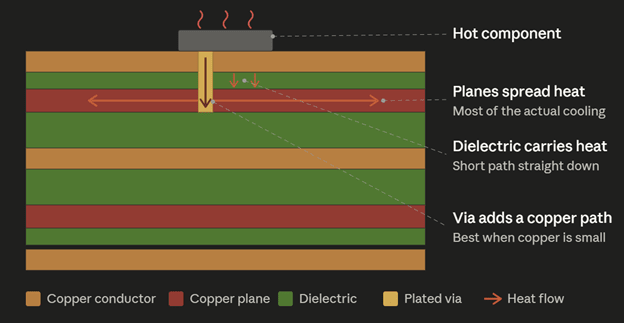
Figure 1: How heat leaves a hot top-side part in an HDI board. Two paths carry heat down to the nearest copper plane: straight down through the thin dielectric over a short path, and through a plated via. The plane then spreads the heat sideways and does most of the actual cooling. Thermal vias help most when the receiving copper is small.
Heat Spreading in Thin Dielectric Cores
Printed circuit boards (PCBs) move heat in two ways. Copper conducts heat very well. Dielectric conducts heat much worse, but it still conducts. Copper has a thermal conductivity around 385 W/m·K. FR-4 dielectric is around 0.3 W/m·K in the through-plane direction. That is a ratio of roughly 1000 to 1.
A common assumption is that dielectric behaves as a thermal insulator . The reality is more interesting. The dielectric layer between a hot pad and a copper plane is the bridge that carries heat from one to the other. Copper is far better per unit area, true. But the dielectric in an HDI buildup has a large bridging area (the whole pad-to-plane footprint) and a short path (2 to 3 mils). So the thin HDI dielectric layers can still contribute meaningfully to vertical heat transfer because of their short conduction distance .
One result from IPC-2152 testing supports this idea. Internal traces run cooler than external traces of the same dimensions. The dielectric around an internal trace pulls heat away better than air pulls heat from a surface trace. This was one of the more surprising findings in the standard.
For HDI designs, this leads to a few useful principles:
Thin buildup dielectrics improve vertical heat transfer. A 2-mil core moves more heat between layers than a 5-mil core, for the same temperature difference across it.
Thin dielectrics also concentrate heat at the next copper layer. The plane below a hot component sees more intense thermal loading. That plane needs to be large enough to spread heat sideways through the copper before passing it down.
Ground planes that serve as references for high-speed signals also work as heat spreaders. This is a useful alignment of purposes. Power planes with splits or cutouts spread heat unevenly, so verify your plane patterns provide adequate spreading in thermally critical regions.
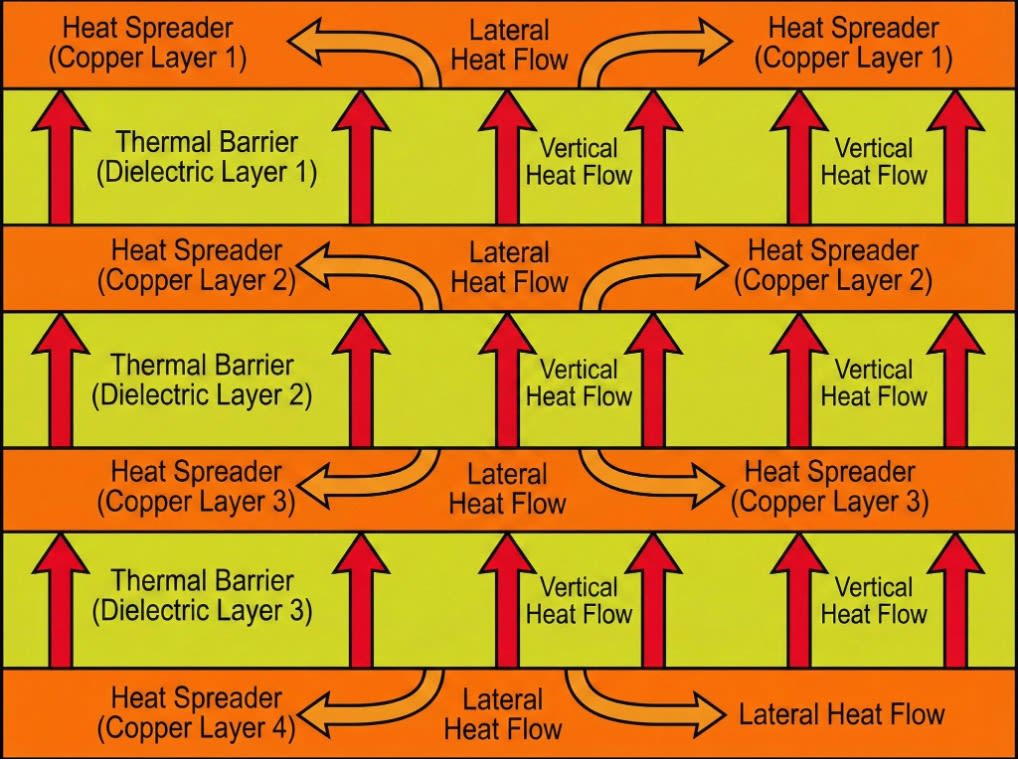
Figure 2: Simplified PCB stackup cross-section illustrating thermal spreading in a multilayer HDI structure. Copper layers provide efficient lateral heat spreading due to high thermal conductivity, while dielectric layers present higher resistance to through-thickness heat transfer. Heat flow in real PCBs is distributed and three-dimensional. Vertical thermal transfer is strongly influenced by vias, copper planes, and local stackup geometry. Via temperature is primarily determined by the surrounding thermal network and connected copper structures, not only by current magnitude.
How Microvia Temperature Actually Works
Most current capacity guidelines treat a via as a stand-alone object. You look up a chart, match the via diameter to a current value, and call it done. Recent research challenges this approach.
In their 2021 book PCB Design Guide to Via and Trace Currents and Temperatures, Douglas Brooks and Johannes Adam used thermal simulation to show that via temperature is often dominated by the surrounding thermal network and connected copper structures rather than via self-heating alone . Via temperature follows the temperature of the parent copper the via connects to.
Steady-state via temperature depends on both resistive heating and the efficiency of the surrounding thermal dissipation path . Copper conducts heat very well. A via sits surrounded by dielectric, much like an internal trace. The parent trace and the receiving copper on the other end act as heat sinks for the via. The via temperature strongly tracks the temperature of the connected copper structures and surrounding thermal environment .
This flips the design question. Instead of asking "how much current can my microvia carry," ask "how is the copper on each end of the microvia behaving thermally?"
A few practical takeaways for HDI design:
A microvia that connects a generous power plane on one layer to a generous power plane on the next will stay cool, even at high current. The connected copper planes dissipate heat efficiently, limiting temperature rise caused by via resistive losses (the heat produced when current passes through resistance).
A microvia that connects a narrow trace to a small pad will run hot, because the connected copper cannot absorb the heat fast enough.
For paralleled microvias under a BGA pad, the cooling comes mostly from the BGA pad and the receiving plane. Adding vias helps when the receiving copper is small. Once the receiving copper is large enough, more vias add diminishing returns. For deeper background on power delivery network design in HDI, the Cadence PDN ebook covers the broader tradeoffs between via inductance, capacitance, and PDN performance.
Stacked microvias add some thermal resistance at each via-to-via interface compared to a single deep via. Each interface is a small but real resistance contribution that adds up across the stack. The dominant factor remains the parent copper at the top and the receiving copper at the bottom.
Copper Balancing to Prevent PCB Warpage
Warpage is the bowing or twisting of the PCB during manufacturing or operation. It results from unbalanced stress states within the board structure. Copper and dielectric expand at different rates under heat. When copper distribution is uneven, differential expansion creates internal stresses that deform the board.
HDI designs face elevated warpage risk due to asymmetric copper distribution. This often comes from dense signal routing beneath components on one surface (often top-heavy), sequential lamination that can lock in residual stress from each cycle, and thin overall board construction that provides less mechanical stiffness to resist bowing.
Copper balancing strategies include:
- Adding copper thieving (dummy fills) in sparse regions to match copper density with dense regions.
- Maintaining symmetric copper percentage between corresponding layer pairs (layer 1 vs. layer N, layer 2 vs. layer N-1).
- Avoiding large copper pours on one side of the board without corresponding copper on the other side.
Most major EDA tools include copper balance analysis features that display copper percentage by layer and by region. Run this analysis iteratively during layout and adjust fills to maintain balance. Target copper percentage variation below 10-15% between corresponding layers.
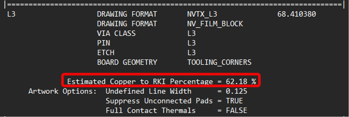
Figure 4: A screenshot or example of a copper balance analysis report from Allegro X PCB Layout showing copper percentage on layer 3 of the NVIDIA Jetson AGX Orin 64 GB - total copper area/route keep-in (RKI) = 62.18% (healthy balance).
When to Combine HDI with Metal-Core or Hybrid Stacks
Some applications demand thermal performance beyond what standard FR-4 HDI can provide. Metal-core PCBs (MCPCB) incorporate an aluminum or copper core layer that dramatically improves in-plane thermal spreading and provides a direct thermal path to heat sinks.
Hybrid HDI-MCPCB constructions place HDI buildup layers over a metal core, providing both the routing density of HDI and the thermal performance of metal-core construction. These designs are common in LED lighting (where high-power LEDs require efficient heat extraction) and in power electronics (where switching devices generate concentrated heat).
Considerations for hybrid construction include CTE mismatch between metal core and dielectric (aluminum CTE ~23 ppm/°C vs. FR-4's in-plane CTE of ~14-18 ppm/°C), via isolation requirements where vias pass through or are adjacent to the metal core, and limited fabricator capability, as not all HDI fabricators offer metal-core hybrid construction.
Alternative thermal enhancement approaches include embedded coin technology (thick copper slugs pressed into the PCB beneath hot components), heavy copper layers (2-4 oz copper vs. standard 1 oz) on planes serving as heat spreaders, and ceramic-filled dielectrics with improved thermal conductivity.
The right thermal enhancement approach depends on power dissipation level, form factor constraints, cost sensitivity, and required reliability. Engage thermal analysis early in the design process to establish requirements before committing to a stackup architecture.
The Sigrity X Aurora Thermal Workflow lets you run thermal analysis directly inside Allegro X PCB Layout during early floorplanning, flagging hotspots and component junction-temperature pass/fail status before the design is locked in. Catching thermal issues at placement is cheaper than catching them at signoff.
A note on sources: the framing of via temperature, thermal vias, and dielectric heat transfer in this revised post draws directly from PCB Design Guide to Via and Trace Currents and Temperatures by Douglas Brooks and Johannes Adam (Artech House, 2021). Thanks to Dr. Johannes Adam for commenting on the original version of this article and pointing out where the conventional framing falls short. The book is the most direct treatment of these topics I've found and is worth reading in full if you design boards where thermal performance matters.