The Physics of Resin Flow: Glass Weave Locking & Dielectric Behavior in HDI Laminations
HDI fabrication success depends on understanding the material physics of lamination. When prepreg is heated under pressure, resin flows to fill gaps, bond layers, and encapsulate copper features. Glass weave provides mechanical reinforcement and dimensional stability.
The interplay between resin flow, glass weave architecture, and process parameters determines whether the finished board meets specifications, or develops defects that compromise reliability. This post examines the physics governing these behaviors.
Resin Flow During Multilayer Lamination
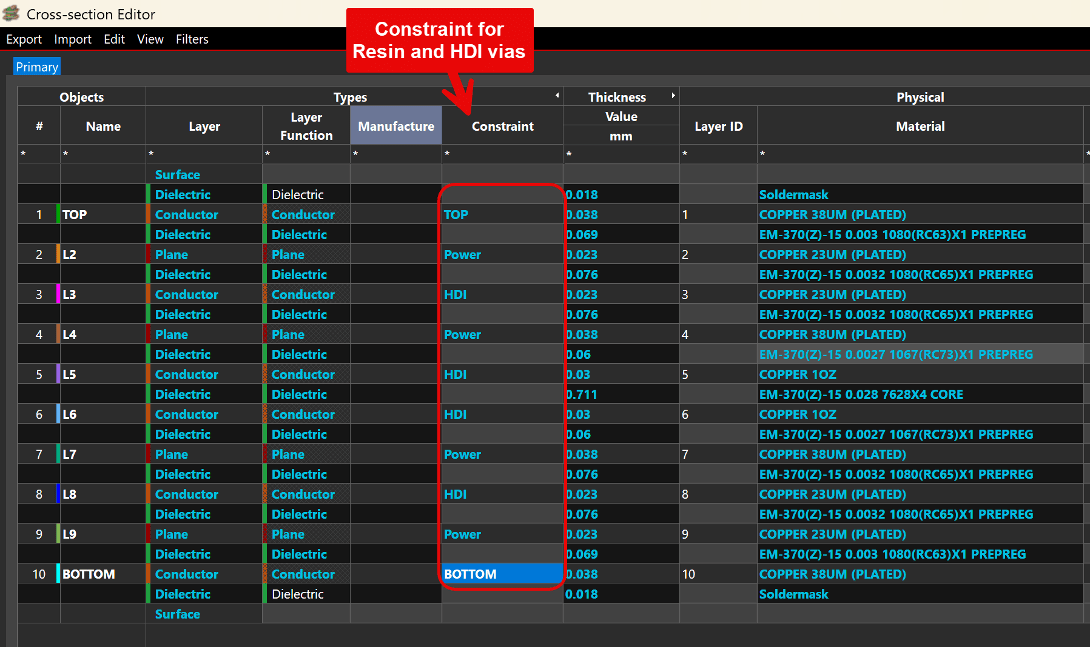
Figure 1: Cross-Section Editor (Setup > Cross-Section) showing a multilayer HDI stackup with prepreg and core layers labeled, including dielectric thickness values in Allegro X.
Prepreg consists of glass fabric impregnated with partially - cured ("B-staged") resin. During lamination, heat softens the resin, reducing its viscosity; pressure forces the softened resin to flow into gaps, around copper features, and into any unfilled via cavities.
Resin flow follows predictable physics. The flow rate depends on resin viscosity (which decreases exponentially with temperature), applied pressure, and flow path geometry. Narrow gaps between closely-spaced copper features resist flow more than open areas. Resin must flow from high-pressure regions (typically the center of large pours) toward low-pressure regions (edges, gaps, and vias).
As the lamination cycle progresses and temperature increases, resin viscosity continues to drop - but eventually the resin begins to crosslink and cure, rapidly increasing viscosity and ultimately solidifying. The process window during which resin can flow is limited; if resin doesn't reach all required locations before cure begins, voids result.
Sequential lamination complicates this picture. Each lamination cycle partially consumes available resin flow. Prepreg that has already flowed in an earlier cycle contributes less flow in subsequent cycles - the resin is partially cured and less mobile. HDI designs with 3-N-3 or deeper stackups may require high resin content prepregs or additional prepreg plies in later lamination cycles to ensure adequate fill.
Glass Weave Orientation Effects on HDI
Glass fabric in prepreg and laminate consists of woven glass fibers in warp (machine direction) and fill (cross-machine direction) orientations. The weave pattern creates a periodic structure with glass bundles and resin-rich gaps between bundles.
This periodic structure affects electrical performance in two ways:
- Dielectric constant variation: Glass has Dk around 6-7; resin has Dk around 3. A trace routed over a glass bundle sees different effective Dk than a trace over a resin-rich gap. This variation creates impedance non-uniformity along the trace length.
- Differential skew in paired signals: If the positive and negative traces of a differential pair align differently with the glass weave - one over glass, one over resin, their propagation velocities differ, creating skew. At multi-gigabit data rates, this "fiber weave effect" can cause significant timing skew.
HDI designs using thin dielectrics are particularly susceptible because fewer glass layers average out the weave pattern. Mitigation strategies include routing traces at angles to the glass weave (commonly 11° or 45°) so both traces in a pair experience similar average Dk, specifying spread-glass or flat-glass fabrics that have more uniform glass distribution, and using resin-coated copper (RCC) buildup layers that contain no glass weaves.
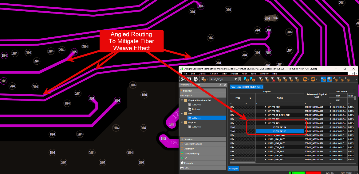
Figure 2: 11 degree angled routing to not only maintain matching signal propagation speeds on both diffpairs, but to reduce fiber weave effects.
Causes of Entrapment, Bubbles, and Delamination
Several defect mechanisms relate to resin flow and lamination physics:
Air entrapment: Air trapped between layers during layup must escape during lamination or be absorbed into the resin. If resin viscosity drops too slowly (insufficient temperature) or cure begins too quickly, trapped air remains as voids. Vacuum-assisted lamination reduces entrapment by removing air before resin flow begins.
Moisture-induced voiding: Moisture absorbed into prepreg or core materials vaporizes at lamination temperatures, creating bubbles. Proper material storage (controlled humidity) and pre-lamination baking of moisture-sensitive materials prevent this mechanism.
Resin starvation: Insufficient resin to fill all gaps leaves voids in starved regions. Most common in areas with dense copper features that displace excessive resin volume. DFM analysis should flag high-copper-density regions at risk for starvation.
Delamination: Separation between layers results from inadequate bonding during lamination (too little resin flow, insufficient temperature or pressure), contamination at interfaces, or stress that exceeds bond strength during subsequent processing or operation. Sequential lamination increases delamination risk because each cycle stresses previously-bonded interfaces.
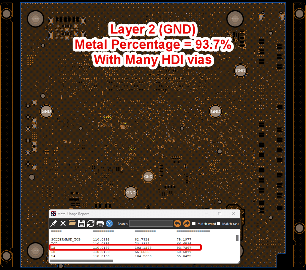
Figure 3: Layer 2 of a high-density PCB with many HDI vias that create resin starvation problems in certain PCB layers and pockets.
Dielectric Constant Variability in Thin Stacks
Controlled impedance design depends on predictable dielectric constant. But Dk varies with resin content, glass style, temperature, frequency, and moisture content. In conventional PCBs with multiple prepreg plies per dielectric layer, these variations tend to average out. In HDI with single-ply thin dielectrics, variation has more impact.
Sources of Dk variation in thin HDI dielectrics include glass weave effects (discussed above), resin content variation from manufacturing lot variations, lamination press-out variation (how much resin flows during lamination), and local copper density effects (more copper adjacent to a trace increases effective Dk through field fringing).
Designers should account for Dk variation when establishing impedance targets. Rather than designing to exact nominal Dk, design with margin for expected variation. Material suppliers publish Dk tolerance specifications; use these in impedance calculations to verify that trace geometries meet impedance targets across the expected Dk range.
For the most demanding applications, consider specifying low-Dk-variation materials specifically designed for controlled impedance consistency. These materials use engineered glass styles and controlled resin content to minimize Dk variation, typically at a cost premium over standard laminates.
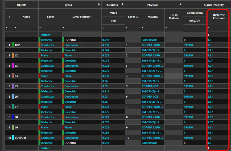
Figure 4: Showing PCB stackup settings in Cadence Allegro X, where one specifies the Dielectric Constant Dk to appropriate values.
Understanding these material physics enables designers to specify appropriate materials, set realistic tolerances, and work effectively with fabricators to achieve reliable HDI builds. The physics don't change, but designs that account for them succeed where designs that ignore them fail.