How to Use Verified Symbols, Footprints, and 3D Models for New Components in OrCAD X CIP
Access to accurate, verified symbols and footprints is essential for efficient PCB design. Manually creating and validating models for complex components can slow design progress, introduce library inconsistencies, and create downstream layout or manufacturing risk. OrCAD X Component Information Portal (CIP) integrates directly with Ultra Librarian, helping teams find pre-built schematic symbols, footprints, and models for new parts while keeping component data connected to the design database.
This quick how-to provides step-by-step instructions for associating and using Ultra Librarian content for new database components in CIP. By pulling verified model data into the component workflow, designers can reduce manual entry, improve library reuse, and continue schematic development with greater confidence.

Opening CIP
Step 1: In OrCAD X Capture CIS, select CIP > Open CIP from the menu.
Step 2: If necessary, log in with your username and password.
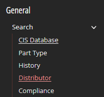
Step 3: Select Search > Distributor from the CIP sidebar menu.
Searching for a New Part
Use the distributor search to locate a manufacturer part number and review available component data before adding the part to the engineering component library. This helps ensure the component record includes the right parametric and sourcing information before model association begins.
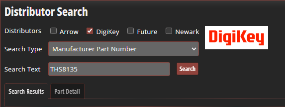
Step 4: Check DigiKey as the distributor.
Step 5: From the Search Type drop-down menu, select Manufacturer Part Number.
Step 6: In the Search Text field, type THS8135.
Step 7: Select Search.
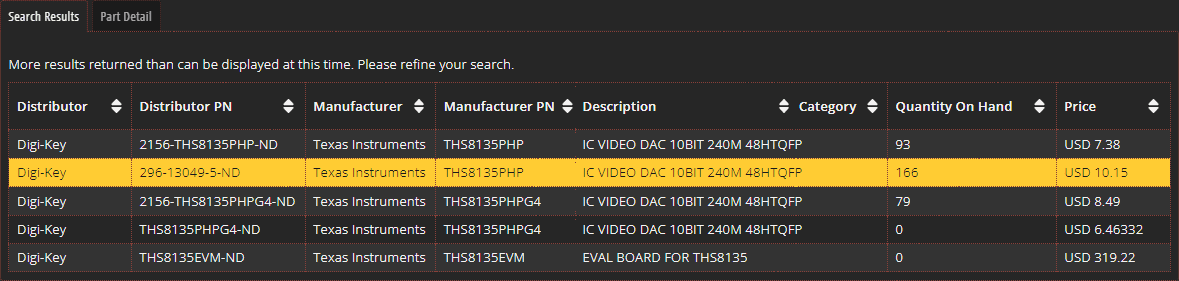
Step 8: From the returned search results, select one of the reported components listed as IC VIDEO DAC.
Accessing Ultra Librarian through CIP
After selecting the part, review the available component information and verify that the associated models match the design requirements. This is especially important for PCB footprints, where pad geometry, package dimensions, and model accuracy directly affect placement, assembly, and manufacturability.
Step 9: Review the component information.
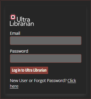
Step 10: In the Ultra Librarian login, enter your username and password and select Log in to Ultra Librarian.
Note: For new Ultra Librarian users, select the Click Here in the Ultra Librarian section to be brought to the registration page.

Step 11: Under the Ultra Librarian integration, select Preview.
Step 12: View the preview of the symbol, footprint, and 3D Model.
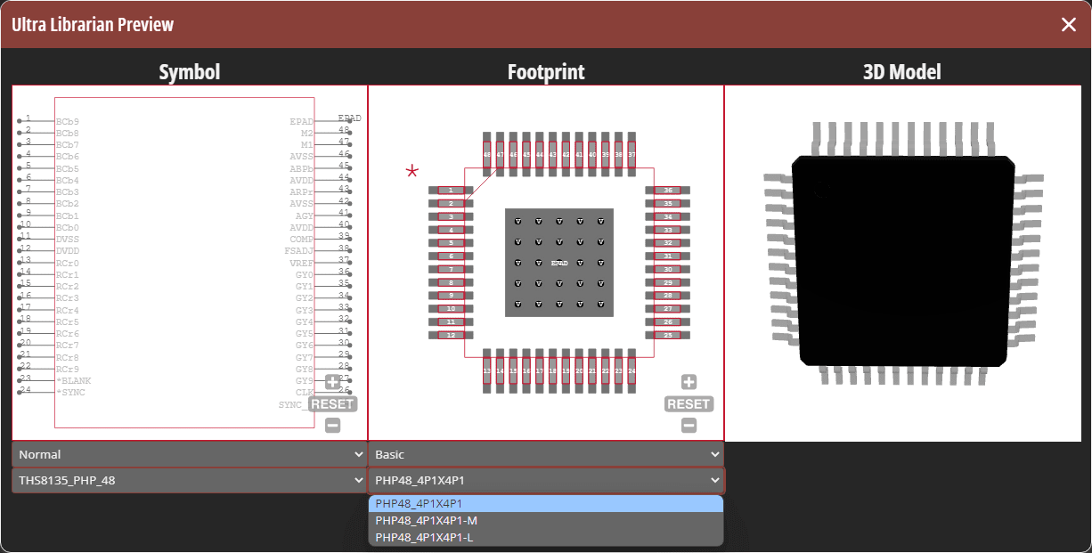
Step 13: For the footprint, select the drop-down menu under Basic to view the additional footprint configurations.
Note: Alternate footprint configurations are available for preview and download for minimum, typical, and maximum pad sizes for footprints according to IPC specifications. When selecting between these options, align the footprint choice with your assembly requirements, internal library standards, and applicable PCB footprint design guidelines.
Some components have additional schematic symbols, for example, larger parts with similar enough sections.
Step 14: For the 3D model, click and drag to rotate the component.
Step 15: Click the X or Close to close the preview.
Adding a Component to the Database
Once the Ultra Librarian models have been reviewed, add the component to the appropriate CIP view so the symbol, footprint, 3D model, parametric data, and distributor information can be managed as part of the component record. This keeps model association and part metadata together, which helps reduce duplicate library work and supports more consistent reuse across projects.
Step 16: Select the Component View drop-down menu and choose ICs.
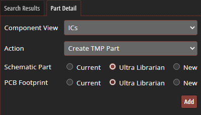
Step 17: Under Action, leave the default Create TMP Part.
Step 18: Under Schematic Part, select the UL radio button.
Step 19: Under PCB Footprint, select the UL radio button.
Step 20: Select Add.
If No Library Folders Are Found
Note: If you receive an error that no library folders are found, Ultra Librarian needs to be configured by an administrator using the following steps:
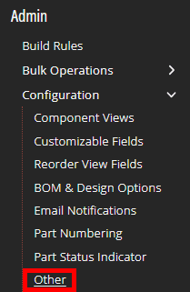
1. Select Admin > Configuration > Other from the CIP menu.
2. Under Ultra Librarian Configuration Directory, select the pencil to edit.
3. Check Enable Common Directory.
4. Set the Common Directory paths for Symbols, Footprints, Padstacks, and Step Models.
5. Check Save Schematic Symbols to Single OLB.

6. Provide a name for the library, such as UL.OLB.
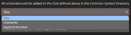
7. Under Duplicate Symbol Handling, click the drop-down menu and select the desired action. Admins can choose from:
- Select "Skip" to skip the Symbol Generation for duplicate symbols
- Overwrite to overwrite the current symbol with the new symbol
- Append a number to add the duplicate symbol with the addition of a number in the name.
8. When finished, select the check mark next to Ultra Librarian Common Directory Settings to save the configuration.
Viewing the Component
After the component is added, verify that each model association is mapped correctly before placing the symbol in the schematic. The preview workflow gives designers a quick way to confirm model integrity and reduce the risk of placing incomplete or mismatched component data.
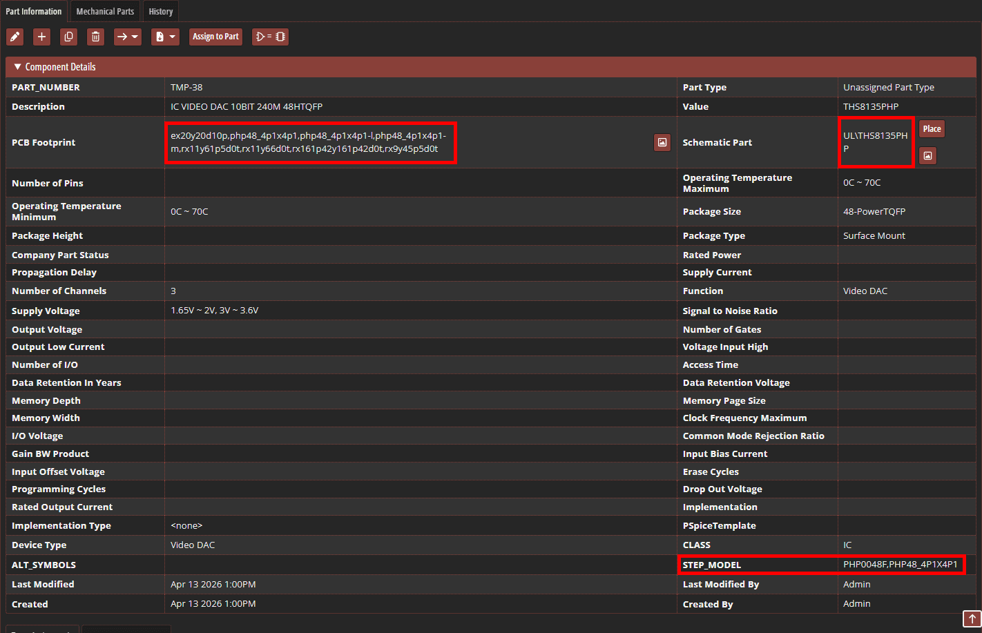
Step 21: View the temporary component. The symbol, footprint, and 3D model have been automatically assigned along with the parametric and distributor information from DigiKey.

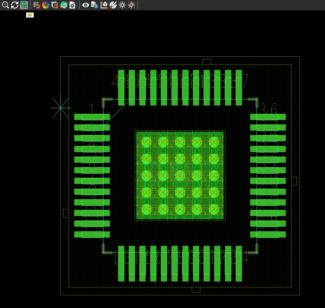
Step 22: Select the PCB Footprint Preview button and click Preview.
Note: If the footprint preview is not configured, select CIP > Settings from the menu. Set the Footprint Viewer Exe to: C:\Cadence\SPB_ [version]\tools\bin\allegro_free_viewer_classic.exe.
Step 23: In the PCB canvas, select the 3D icon on the toolbar to view the pre-mapped STEP model.
Step 24: Leave the defaults in the 3D Canvas Filter and click OK.
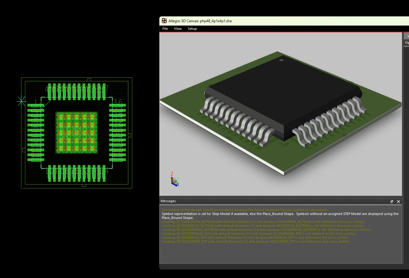
Step 25: View the PCB Footprint and 3D Model.
Step 26: Close the 3D Model and PCB footprint preview.
Step 27: Select the Symbol Preview button.
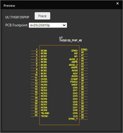
Step 28: View the schematic symbol preview.
Note: If the symbol has multiple sections, select the letters across the top to see each section.
Step 29: Select the place to place the symbol in the schematic canvas. If additional component edits are needed later, use the available OrCAD workflows for reviewing and updating symbols through Component Explorer or the appropriate library management tools.
Step 30: Click to place the schematic symbol in OrCAD Capture CIS. Right-click and select End Mode or ESC on the keyboard when finished.
Note: The temporary part can be utilized in the schematic while the component is reviewed and approved.
Wrap Up and Next Steps
CIP and Ultra Librarian integration helps accelerate PCB design by connecting part search, verified model access, and database component creation in a single workflow. Instead of manually building every schematic symbol, footprint, and 3D model, designers can preview available models, select the appropriate configurations, and automatically associate them with new database components.
With verified pre-built content mapped to parametric and distributor information, teams can improve component accuracy, reduce duplicate library creation, and keep schematic development moving while components move through review and approval. For teams managing growing libraries, this workflow supports faster part introduction, cleaner database records, and more consistent ECAD model reuse across designs.