Allegro X Advanced Package Designer Silicon Layout Option Datasheet
Fan-out wafer-level package (FOWLP) design places new demands on the IC backend and package substrate design teams and the design tools and flows that they use. The Cadence Allegro X Advanced Package Designer Silicon Layout Option provides a complete design and verification flow for the specific design and manufacturing challenges of FOWLP designs.
Overview
While wafer-level packaging (WLP) is not a new technology or process, as with all technologies, it evolves. In its latest evolution as foundry-driven FOWLP, it provides a number of new advantages for the handheld/mobile/ wireless/multimedia product market segment.
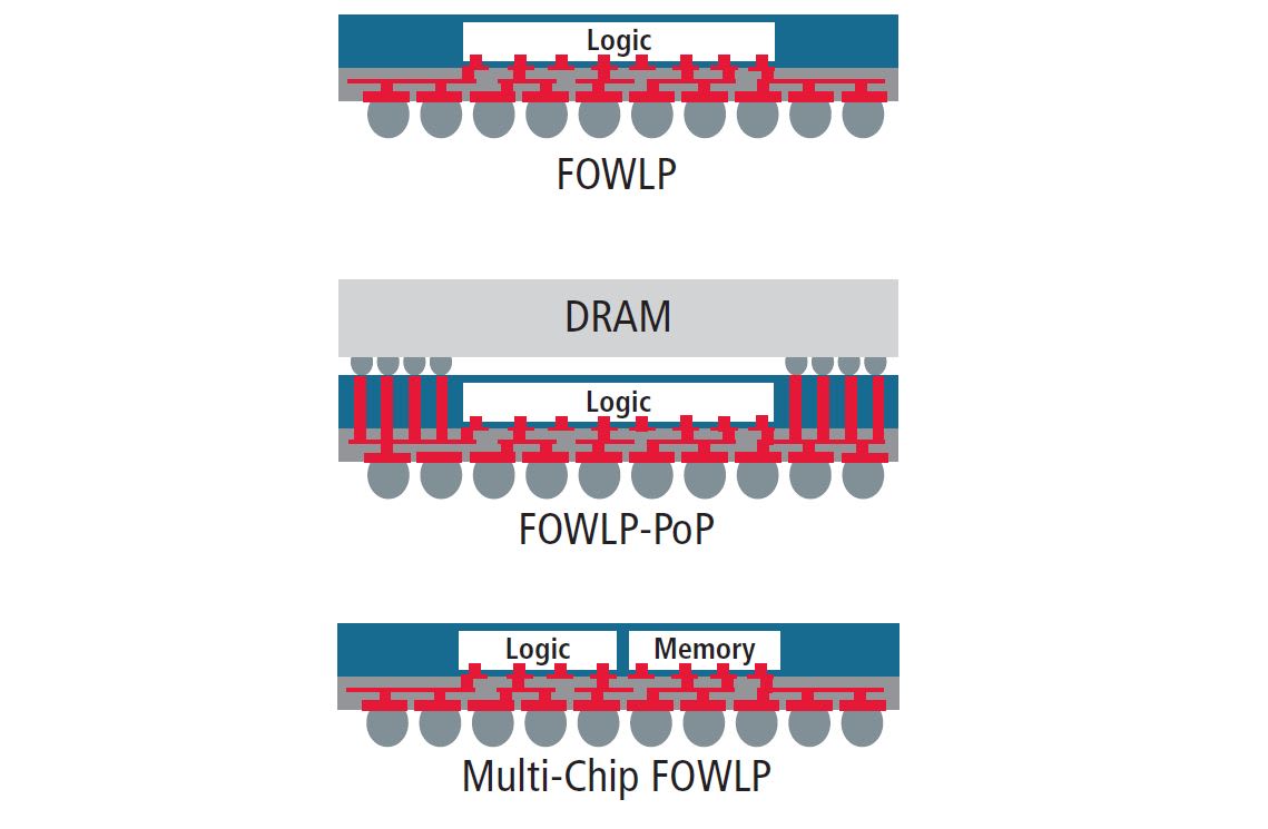
FOWLP technology, based on wafer molding and fine metal processes without substrate, enables the reduced thickness, optimized performance, and lower cost ideal for its initial target market, mobile computing products such as smartphones and tablets. Such devices are evolving at a rapid pace as faster and more powerful multi-core application processors become available. FOWLP enables a thinner PoP stack with better routing density, higher operating frequency (fMAX), higher memory bandwidth DRAM, and better heat dissipation than conventional chip-scale packaging methodologies.
Silicon Layout Option
The majority of these emerging FOWLP designs may fall under the responsibility of the IC back-end design teams of the fabless semiconductor company. However, these designs may also place demands on the IC package substrate designer/teams. The IC packaging design tools must be extended to support the requirements of modern FOWLP designs. Through working with leaders in this emerging segment, Cadence has been able to develop the Silicon Layout Option, which provides a complete design through verification flow for the specific design and manufacturing challenges of FOWLP.
As the Silicon Layout Option uses a wafer-level implementation and process, the path to manufacturing is radically different from that of a typical organic substrate-based IC package manufacturing process. For the Silicon Layout Option, the manufacturing process is the same as, or very similar to, an IC manufacturing process. At the macro level, the differences and challenges from traditional organic IC package manufacture include:
 Figure 1: Examples of FOWLP
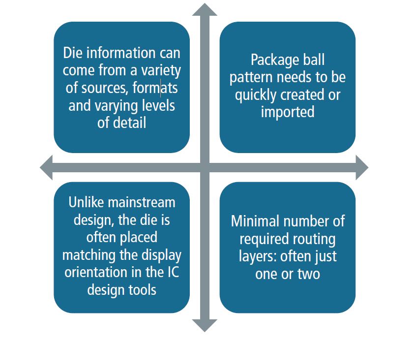
  Figure 2: Some typical design challenges unique to FOWLP implementations that must be managed by design tools and designers
- A process design kit/rules deck (PDK) must be used, followed by verification signoff
- Specific interconnect (metal) must follow foundry/fabricator rules and techniques common in IC design and fabrication
- GDSII or Stream is the path to mask creation for the FOWLP manufacture
- PDK-adherence verification/signoff is required before a design/mask enters manufacturing
Features
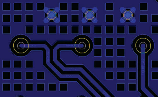
Figure 3: Metal creation and management tools allow the designer to scan, assess, and modify the localized metal density on each layer to meet the foundries’ stringent fabrication requirements on both shapes and pads
The Silicon Layout Option in conjunction with the Cadence Physical Verification System (PVS) enables designers to address these macro-level items. Some of the features specific to the Silicon Layout Option are:
- Localized, tightly controlled metaldensity creation and editing tools to control warpage in ultra-thin packages (500 to 1000µm)
- Metal-density utilities for across-design balancing with meshed metal and meshed pads
- High-performance GDSII mask processing
- Direct integration with PVS for design and mask verification and signoff to PDK rules deck
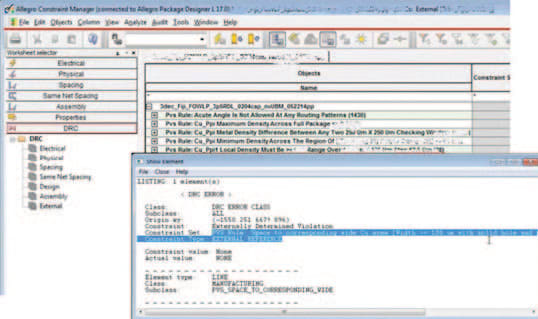
- PVS verification issue highlighting and reporting directly on design canvas and in constraint manager
Platforms
The Allegro X Advanced Package Designer Silicon Layout Option is available with Allegro X Advanced Package Designer and is designed to be used in conjunction with the Cadence PVS, which must be purchased separately. The Silicon Layout Option is available in these versions:
- Windows (64 bit)
- Linux (64 bit)
Figure 4: Foundry-supplied PDK / rules-deck-driven PVS verification results are directly displayed with the SiP Editor using the constraint manager
Cadence Services and Support
- Cadence application engineers can answer your technical questions by telephone, email, or internet—they can also provide technical assistance and custom training.
- Cadence-certified instructors teach more than 70 courses and bring their real-world experience into the classroom.
- More than 25 Internet Learning Series (iLS) online courses allow you the flexibility of training at your own computer via the internet.
- Cadence Online Support gives you 24x7 online access to a knowledgebase of the latest solutions, technical documentation, software downloads, and more.
- For more information, please visit support and training

