Integrity System Planner Datasheet
System-level design planning and optimization from silicon through IC packaging to PCB
Cadence Integrity System Planner revolutionizes the system-level interconnect architecting, assessment, implementation, and optimization process by unifying IC, interposer, package, and PCB data in a single environment where signal-to-bump/ball assignment and connectivity/routing pathway scenarios are easily derived and evaluated in the context of the complete system prior to implementation. Full-system connectivity visualization and a unified data model enable rapid exploration and propagation of changes to adjacent substrates, providing instantaneous feedback on their system-wide impact. The system design can be used as the basis for system-level analysis, such as system LVS, thermal, power, and signal integrity. Integrity System Planner helps engineers or architects achieve the right balance of multi-substrate interconnect integration for optimal performance, cost, and manufacturability before implementation—resulting in fewer iterations and shorter cycle times.
Overview
Integrity System Planner helps design teams optimize device and system performance by providing a single environment for architecting, evaluating, and driving connectivity across the multiple substrates that comprise the system. It is ideal for system architects, project leads, or individual designers responsible for developing the die-to-die, die-to-package/interposer, or package-to-PCB interface, and coming up with the optimal combination of bump/ball configurations and signal assignments. A key differentiator for Integrity System Planner is the ability to maintain the individual integrity and extent of each design while providing a complete system view and interoperability, as shown in Figure 1. Each design can be prepared and managed for the appropriate implementation environment. System-level analysis can be configured and launched from the Integrity 3D-IC System Platform , Cadence’s high-capacity, unified design and analysis platform for designing multiple chiplets.
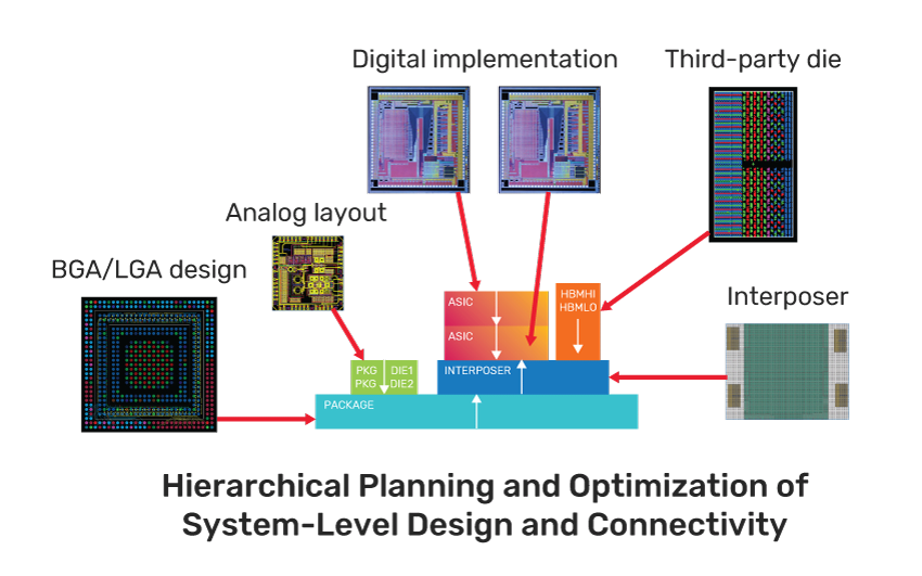 Figure 1: Assemble and manage system design
Benefits
- Correct-by-construction single-source system design
- Optimized inter-substrate connectivity and bump assignment
- Increased performance with reduced overall wire lengths
- Reduce routing layers and vias with optimized connections
- Reduce ECO cycle time and complexity
Features
System-Level Assembly and Planning
Integrity System Planner provides an environment capable of uniting design content from various sources for the purpose of system-level design assembly, floorplanning, connectivity definition, and optimization (Fig. 2) and communicating that data to their respective implementation tools for completion. It is part of an overall cross-substrate solution that provides interoperability across a range of Cadence products, including Cadence Innovus Implementation System and Cadence Virtuoso Studio. In addition, package designs developed in Integrity System Planner can be directly imported into the Cadence Allegro Package Designer Plus environment to help expedite detailed package implementation. In this way, the entire system design can be created and managed through implementation from a single source. The ability to visualize system-level connectivity coupled with connectivity optimization features enable bump optimization throughout the system.
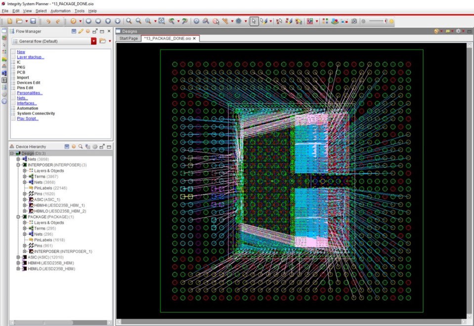 Figure 2: System-level connectivity definition, visualization, and optimization
Contact Layer Definition and Management
An initial step in cross-substrate optimization is establishing the physical relationships between the die, package, interposer, and PCB (devices). The contacting pad layers from each device are identified to establish a physical connection, and mating contact pads can be automatically created on the contacted device. Integrity System Planner automatically manages these relationships and maintains the integrity of the contact pads on each substrate through design updates, as shown in Figure 3.
 Figure 3: Configure design stack
Creating contact layers also establishes a logical relationship between the devices. Nets are automatically propagated to the contacted device as a result of the contact pad definition. Net name prefixes uniquely identify net names for replicated die, such as high bandwidth memory (HBM)s. Nets can then be mapped to establish connectivity between devices with differing net names.
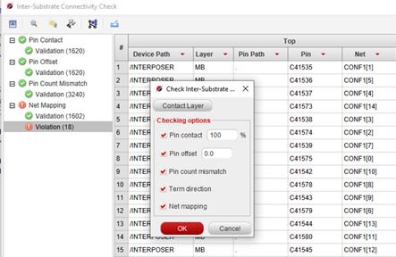
Inter-substrate connectivity checks, such as shown in Figure 4, are performed to verify the integrity of the contact layers. Checks include pin contact percentage, pin offset, pin count mismatch, term direction, and net mapping. Violations are listed, and offending objects can be highlighted. This capability helps keep the system design connectivity intact throughout the design process.
Figure: 4 Inter-substrate connectivity checks
Connectivity Definition and Optimization
As a flexible exploration environment, Integrity System Planner works with an existing netlist, without a netlist, or as in most cases, with a partial netlist. The Netlist Editor feature allows the designer to propagate and map nets up and down the logic hierarchy, as shown in Figure 5. Connectivity can be defined by interactively mapping nets using regular expressions to define patterns. Nets are automatically propagated between substrates as a result of the contact pad creation or the connection optimization process. Connectivity can also be defined by importing a CSV net mapping file, CSV Term file, or Verilog netlist.
 Figure 5: Interactive net mapping and visualization
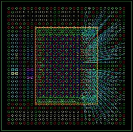
The Connectivity Optimization feature enables automated pin assignment to reduce route crossings and net length. This feature can be used to optimize die-die connections or top-side bumps/pads to bottom-side bumps/balls, as shown in Figures 6 and Figure 7.
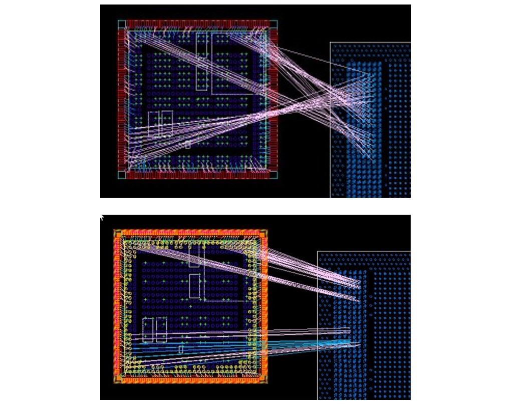 Figure 6: Die-to-die connectivity optimization
Figure 7: Optimized bottom-side bump assignment
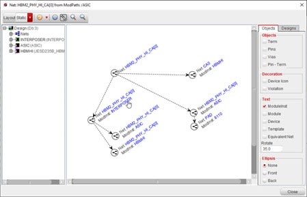
System-level connectivity can be analyzed using either the Netlist Editor feature or the Net Graph feature. Net Graph shows the entire topology of the net, including mapped child net names, terms, pins, and vias that exist on the net, as shown in Figure 8.
Figure 8: Explore net topology across the system design
Implementation Integration
Integrity System Planner is well integrated with Allegro Package Designer Plus. Databases are imported directly into Allegro Package Designer Plus to produce the symbols, layer stackup, padstacks, and netlist needed for implementation. Incremental changes can be made in Integrity System Planner and imported into the active Allegro Package Designer Plus design. Changes made in the Allegro environment, such as pin swaps, part placement, etc., can be merged back into the Integrity System Planner source design to keep them in sync.
Integrity System Planner is also the cockpit for the Integrity 3D-IC platform, providing tight integration with Innovus Implementation System, Virtuoso Studio, and Allegro Package Designer Plus.
Interface Formats
- Chip data: Die Abstract, Library Exchange Format (LEF)/Design Exchange Format (DEF), die TXT, and pin CSV files
- Package data: Direct data exchange with Cadence Allegro (.sip, .mcm), die TXT, pin CSV files, and Die Abstract
- PCB data: Cadence Allegro PCB (.brd) and other popular systems
