When Do Layout Decisions Become SI Problems?
Signal integrity (SI) failures rarely come from one big mistake. They build up from a series of layout decisions that each seemed reasonable at the time. You chose a via type. You routed a differential pair across a few layer transitions. You accepted the default stackup material. Each of those decisions changed the electrical behavior of your signals. And by the time you run analysis or build the first prototype, the combined effect shows up as timing failure, excessive noise, or a failed eye diagram.
The root cause is almost always in the layout, not the schematic. The schematic defines what connects to what. The layout defines how those connections behave electrically. Three layout decisions have the largest impact on signal quality: routing topology , via strategy, and stackup material choice.
Decision #1: Your Routing Choices Determine Signal Behavior
Every high-speed signal travels as a wave along a transmission line. That wave needs two things: a forward path (the trace) and a return path (the reference plane underneath). The return current flows on the reference plane, directly under the trace, at the same speed as the signal. This is how energy moves through a printed circuit board (PCB).
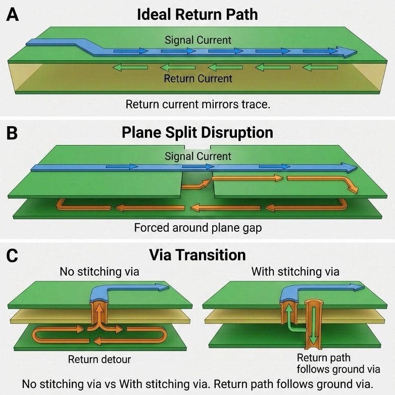
Figure 1: Return path comparison depending on PCB routing. A. Ideal return path geometry allows for an adjacent return path through tight displacement current, B. Gap in adjacent plane produces fields to take a long path to adjacent return plane, C. How return path stitching vias affect return path
When a signal changes layers through a via, the return current must also change reference planes. If there is no nearby ground via to provide that transition, the return current must find another path. It spreads out, travels farther, and increases the loop area. That increased loop area adds inductance to the signal path. Inductance slows edges, creates voltage spikes, and increases electromagnetic emissions.
This is a routing topology problem. Two differential pairs on the same board, with the same stackup and the same driver ICs, can have completely different signal quality based on how they are routed. A differential pair that stays on two layers and changes reference planes once will have a clean return path. A differential pair that crosses nine layers and four reference planes will have a return path full of discontinuities.
The Sigrity X Aurora Return Path workflow visually highlights the issues within your design. On a test design, two USB differential pairs were routed on the same board. The first pair (P0_USB) changed two layers and maintained a clean return path with high quality. The second pair (P1_USB) changed nine layers across four reference planes before returning to the top layer. The return path quality difference between these two circuits was large, even though both passed the standard design rule checks (DRCs). Routing decisions created the difference.
Decision #2: Your Via Choice Sets a Frequency Limit on the Signal
When a signal transitions from one layer to another through a plated through-hole (PTH) via, the via extends through the entire board thickness. The portion of the via below the target layer is called the stub. This stub is a dead-end conductor. The signal does not use it, but electromagnetic energy still enters it.
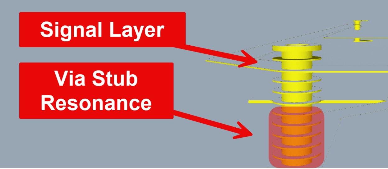
Figure 2: Via stub resonance concept. Cross-section showing a PTH via with the stub portion highlighted below the target signal layer. Removing these stubs reduces EMI field effects from spreading wherever they please.
Energy travels down the stub, hits the open end, and reflects back. At a specific frequency, the round-trip delay through the stub equals half the signal wavelength. At that frequency, the reflected energy cancels the original signal. This creates a resonance dip in the frequency response, which means the signal loses power at exactly that frequency.
The frequency where this happens depends on the stub length, the dielectric constant (Dk) of the board material, and the full 3D geometry of the via structure (pad size, antipad clearance, ground via distance). A longer stub resonates at a lower frequency. A higher Dk also lowers the resonant frequency because signals travel slower in higher-Dk materials. In Advanced Signal Integrity for High-Speed Digital Designs (Thierauf), a full-wave 3D electromagnetic simulation of a 37.8-mil via stub showed resonance around 10 GHz.
At that resonant frequency, roughly 62 percent of the signal power radiated into the surrounding plane layers rather than reaching the receiver. The authors note that simple quarter-wave formulas only approximate the actual resonance within a few gigahertz, because the parasitic capacitance and inductance of the physical via structure shift the resonant point. The takeaway is practical: if your signal bandwidth gets anywhere near the stub's resonant frequency, the stub needs to be shortened or removed.
This is why via type matters. Blind vias, buried vias, and back-drilled vias all reduce or remove the stub. A blind via that connects Layer 1 to Layer 3 has no stub below Layer 3. A back-drilled PTH via has its stub physically removed after plating. Choosing the right via type for your signal frequency sets the upper limit on the usable bandwidth of the channel.
Decision #3: Your Material Choice Controls Signal Speed and Loss
The stackup material affects every signal on the board. Two properties matter most: the dielectric constant (Dk) and the dissipation factor (Df), also called loss tangent.
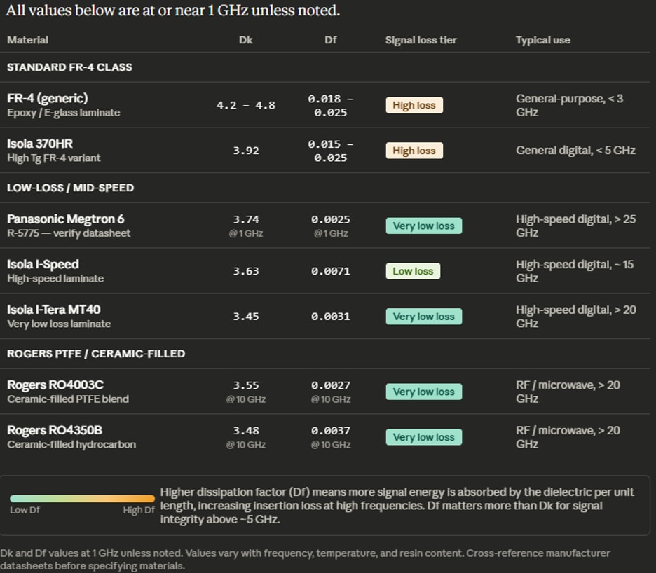
Figure 3: Material comparison table showing approximate Dk and Df values for FR-4, Megtron 6, Isola I-Speed, and Rogers materials across various sources for reference only, and not for design. Specifically for Panasonic Megtron 6, material values may vary, as they change their specs often. Please verify all values on this table with the manufacturer before specifying materials. Cadence and the author are not responsible for design errors caused by not verifying the above information with the manufacturer in your specific use case.
Dk controls signal speed and impedance. A higher Dk slows the signal and changes the impedance relationship between trace width and dielectric thickness. If you change materials from FR-4 (Dk around 4.0) to a low-loss laminate like Panasonic Megtron 6 (Dk around 3.63), the impedance changes for the same trace geometry. Your trace widths need to be recalculated for the new material.
Df controls signal loss at high frequencies. Every time a signal wave passes through the dielectric, some energy is absorbed and converted to heat. Higher Df means more loss per unit length, and the loss increases with frequency. Standard FR-4 (Df around 0.015 to 0.025) works for signals up to a few gigahertz. For faster signals, low-loss materials like Isola I-Speed (Df around 0.007) or Megtron 6 significantly reduce attenuation.
Dk also affects crosstalk. Lower Dk materials reduce the coupling between adjacent traces. The Sierra Circuits HDI Design Guide reports that crosstalk in high-density interconnect (HDI) substrates can drop by as much as 50 percent when using lower-Dk materials combined with shorter coupled trace lengths.
The material choice is made once, in the Cross-Section Editor, and it propagates into every impedance calculation, every loss simulation, and every crosstalk analysis for the entire board.
These Are Layout Decisions, Not Schematic Decisions
The schematic does not specify via types, routing layer transitions, or board materials. Those are layout decisions. And they control whether your signals arrive clean or degraded. Routing topology sets the return path quality. Via strategy sets the frequency limit. Material choice sets the loss floor and the crosstalk baseline.
Each of these decisions can be evaluated during layout using Allegro X PCB Layout with Sigrity X Aurora. You can extract the routing topology, simulate the via structure, and verify the material properties before sending the design to fabrication. The point is to make these decisions with data, not defaults.