How to Simulate PCB Design Using PSpice and OrCAD X
Key Takeaways
-
PSpice allows designers to verify circuit behavior, like switching thresholds, bias points, and expected outputs, directly from the schematic.
-
Integrated impedance and coupling analysis in OrCAD X enhances front-end PCB simulation accuracy.
-
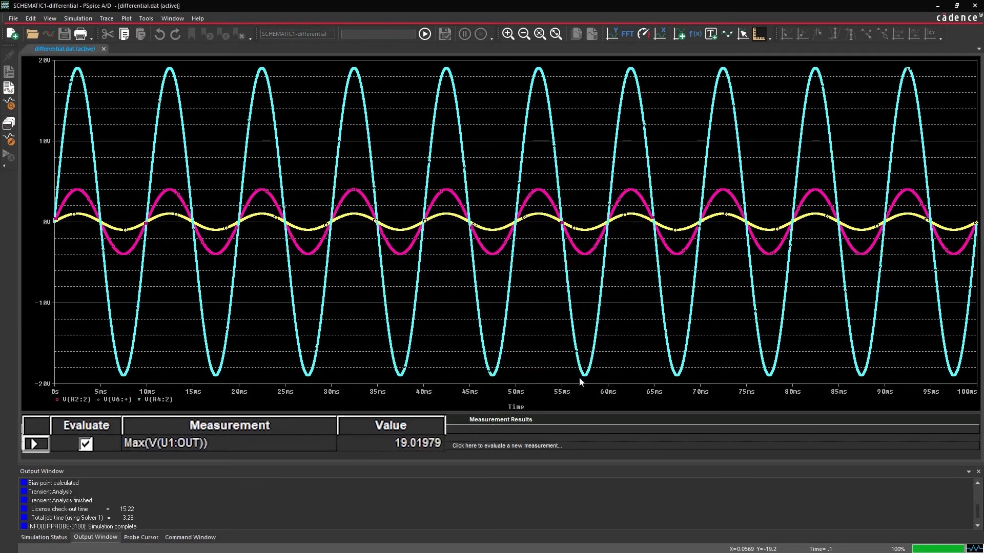
Simulation techniques like FFT, thermal, and transient analysis enable designers to optimize and validate circuit performance in real-world conditions.
When it comes to printed circuit boards, simulation is synonymous with success. It’s not just about verifying a design; it’s about predicting its behavior, identifying potential pitfalls, and ensuring optimal performance before ever etching a board. And that all starts with schematic-level simulation, where PSpice is a powerful ally.
If you’re learning how to simulate your PCB design, schematic simulation is the best place to begin–it's all about catching issues early. Front-end PCB simulation, performed directly on the schematic, allows you to analyze aspects like impedance and coupling before committing to a physical layout.
This is where tools integrated within your design environment—like those integrated into OrCAD X—truly shine. They provide immediate feedback, enabling iterative design improvements with minimal overhead. Think of it as a dress rehearsal before the main performance; you want to iron out the wrinkles before the audience arrives.
Simulation for PCB Design
Simulation is about creating a virtual representation of your circuit and subjecting it to various operating conditions and stimuli. This allows you to observe how the circuit behaves without the time and expense of building a physical prototype.
PSpice is a versatile tool that can be used for both schematic and layout simulation. It offers a wide range of analysis types to suit different design needs. To understand how to simulate PCB design in PSpice, here's a summary of some key analysis types available.
Simulation and Analysis Types
|
Analysis Type |
Description |
When to Use |
|
Time Domain (Transient) |
Simulates the circuit's behavior over time, showing how voltages and currents change with respect to time. |
|
|
DC Sweep |
Analyzes the circuit's response to varying DC input voltages or currents. |
|
|
AC Sweep/Noise |
Analyzes the circuit's frequency response, showing how it responds to different AC frequencies. Noise analysis can also be performed. |
|
|
Bias Point |
Determines the DC operating point of the circuit (voltages and currents at each node). |
|
How to Simulate PCB Design: Schematic-Simulation in PSpice
Building a PSpice Project and Schematic
To begin, you'll need to set up a PSpice project. Here's a quick rundown:
-
New PSpice Project: Start by selecting "New Project" from the start page or the file menu. Check the "Enable PSpice simulation" box. Select "Blank Project" for a clean slate for your schematic.
-
PSpice Components: Navigate to the "Place" menu, then select "PSpice component." From there, you can choose basic components like diodes, inductors, capacitors, and resistors.
-
Searching for Specific Parts: For components like MOSFETs, use the "Search" option within the PSpice component menu. A search window will appear, allowing you to type in the part number (e.g., "IRF840") and select the desired component.
-
Voltage Sources and Ground: Add voltage sources from the "Modeling Applications" submenu. You can configure independent voltage sources with various waveforms (pulse, DC, etc.) using the modeling GUI. And, of course, don't forget to place a ground.
-
Connect your Components: Select the "Wire" icon from the toolbar and carefully draw connections between the component symbols. Below is an example
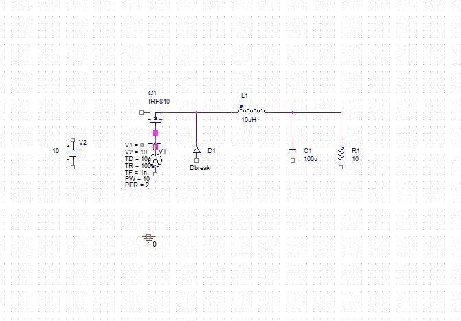
Easily draw connections between your components
Simulation Profiles & Analysis Techniques
Before running a simulation, you need to define a simulation profile. This is where you specify the type of analysis you want to perform and the simulation parameters.
-
New Simulation Profile: Go to the "PSpice" menu and select "New Simulation Profile." Give your profile a descriptive name (e.g., "sim1").
-
Analysis Type: Within the simulation settings GUI, choose the appropriate analysis type. Keep in mind your needs when choosing the four types we discussed above: Time Domain, DC Sweep, AC Sweep, and Bias Point.
-
Run: With your simulation profile defined, it's time to run the simulation. Select the "Run" command from the PSpice menu or toolbar. PSpice will then crunch the numbers and generate the simulation results.
Note that further analysis techniques can be enabled/studied utilizing PSpice:
-
FFT (Fast Fourier Transform): Analyze the frequency content of signals to identify noise sources, harmonic distortion, and signal integrity issues. This can be applied to Time Domain analysis results.
-
Thermal Sweep: While primarily a PCB-level analysis, you can incorporate basic thermal considerations into schematic simulations to identify potential hotspots. This requires component models with thermal parameters.
-
Sensitivity Analysis: Determine which component parameters have the greatest impact on circuit performance. This helps you identify critical components and optimize their values.
-
Monte Carlo Analysis: Perform multiple simulations with randomly varied component values to assess the circuit's robustness to manufacturing tolerances.
-
Instantaneous Changes: Simulate sudden changes (e.g., a load step) to observe how the circuit responds to unexpected events.
-
Parameter Sweeps: Some analysis types allow for sweeping component parameters to observe their effects on circuit performance. This is particularly useful for optimizing component values and understanding design sensitivities.
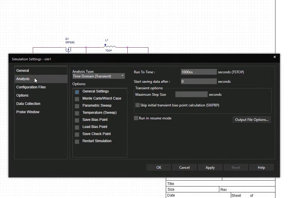
There are many options when configuring your analysis
OrCAD X In-Design Signal Integrity Analysis
Outside of schematic-level simulation in PSpice, OrCAD X features built-in signal integrity (SI) analysis within your PCB layout environment. SI analysis considers the physical characteristics of your design.
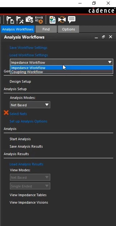
The Impedance & Coupling Workflow
The impedance workflow allows you to analyze the impedance of nets in your design, which assists in preventing signal reflections and maintaining signal integrity.
The coupling workflow analyzes the coupling between nets, which is a precursor to crosstalk. While not a full crosstalk analysis, it's faster to run and easier to set up.
Here's how they work:
-
Net-Based vs. Directed Group: You can choose between "Net Based" and "Directed Group" analysis. Both provide impedance values, but "Directed Group" offers additional reporting, showing the impedance from a source to a receiver.
-
Selecting Nets: In the "Select Nets" form, you can pick the nets you want to analyze. You can choose a "Flat" or "Hierarchical" organization. Hierarchical is often preferred as it breaks down nets based on differential pairs and buses. Unless you're dealing with an exceptionally large design, you can generally analyze all nets without a significant performance hit.
-
Coplanar Traces: For impedance, you can optionally detect and model coplanar traces. Note that this will increase simulation time.
-
Analysis Options: For coupling, specify the rise time and coupling coefficient in the geometry window.
Viewing the Impedance Table and Plots
After the analysis, you can view an impedance table with two tabs: "Single Ended Impedance" and "Differential Impedance." The table includes columns for the number of vias, reference planes, min/max/typical impedance, length at min/max/typical impedance, total length, and delay. You can sort by impedance values (e.g., max impedance) to identify nets of concern.
Interpreting Coupling Visions and Tables
After the analysis, you can enable "Coupling Visions" to overlay the coupling results on the layout. This color-codes the nets based on the coupling coefficient, highlighting areas with high coupling. You can switch between "Worst Case" and "Victim Net" views to focus on the most problematic nets or the nets most susceptible to crosstalk.
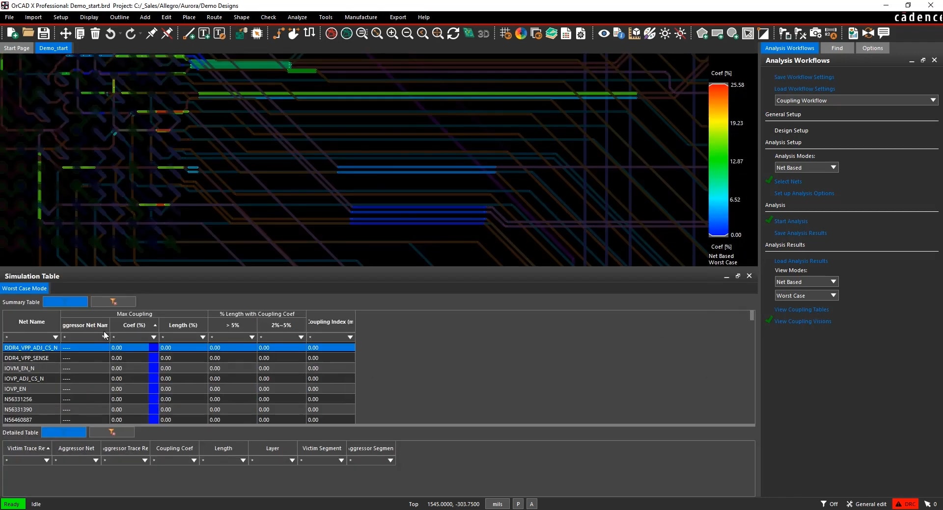
Find the most coupled segments in your design
Ready to elevate your design confidence? Learning how to simulate your PCB design effectively leads to reliable, high-performance boards. With Cadence tools like OrCAD X and PSpice, designers gain access to powerful schematic-level simulations and integrated in-design analysis options. From transient response and FFT to thermal behavior and impedance analysis, these tools help engineers predict and resolve issues early—before layout or prototyping. Try it yourself with a Free Trial of OrCAD X and experience the power of simulation.