Grounding and Return Paths: Essential for High-Speed Designs - Part 1
Why Proper Grounding Makes or Breaks Your High-Speed PCB Design
Proper grounding is crucial for ensuring signal integrity in high-speed PCB designs. Current flows from the power source through supply rails and components, then returns through the ground plane to complete its circuit. This fundamental principle matters a lot in high-speed designs.
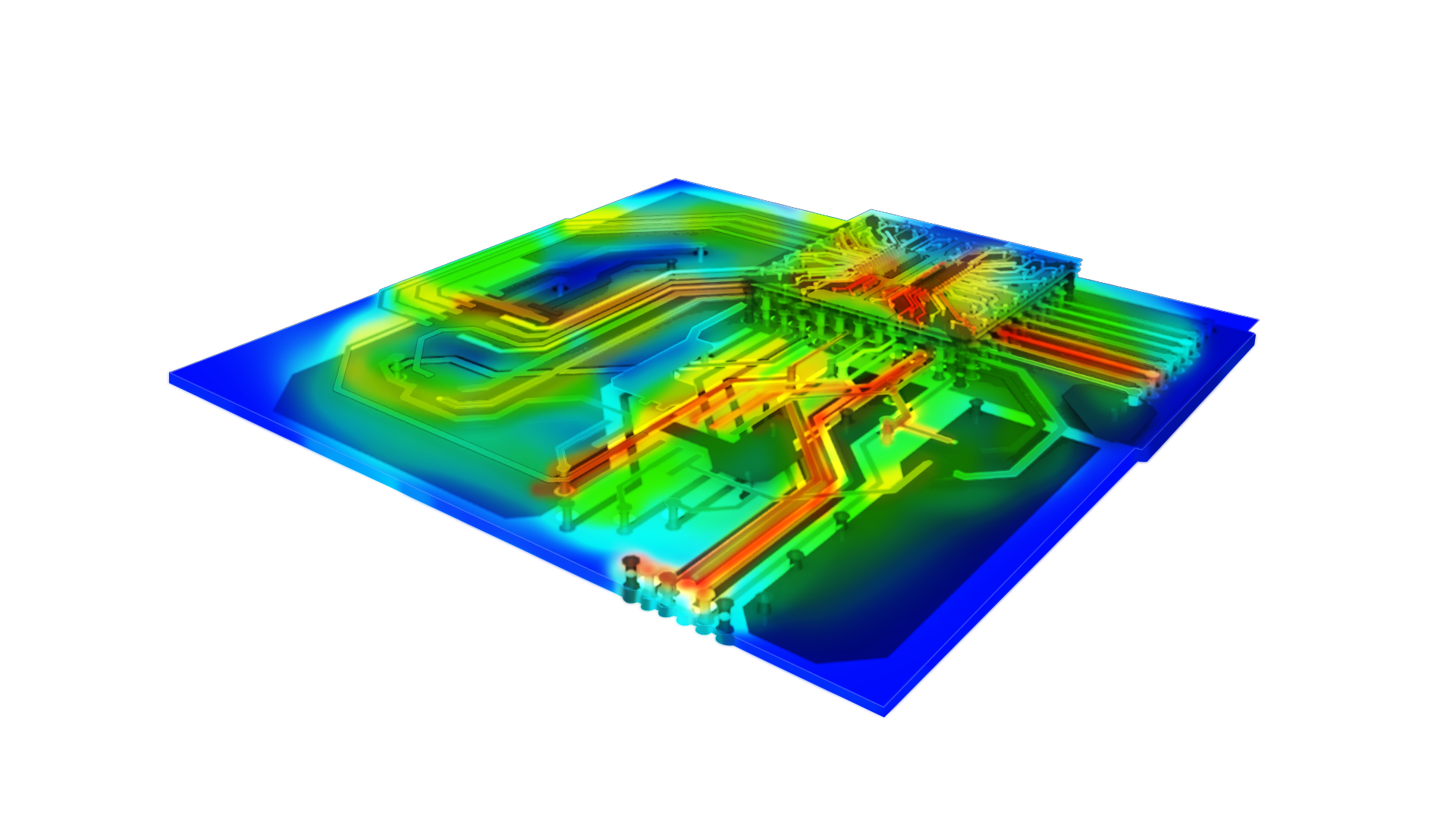
At high frequencies, particularly in the MHz range and above, return current follows the path of least impedance, creating complex distribution patterns beneath signal traces. Effective PCB grounding relies on techniques such as dedicated ground planes and smart via placement. Separating high- and low-voltage sections with individual ground planes is also essential to reduce crosstalk in high-density boards.Our experience confirms that these approaches are the foundation of reliable electronic designs.
Understanding the importance of proper grounding strategies can differentiate between success and failure in high-speed PCB design. This article highlights common pitfalls and provides practical ways to maintain signal integrity. It covers specific techniques, such as optimal bypass capacitor placement and ground plane implementation, equipping you with the knowledge to achieve reliable circuit performance.
Common High-Speed PCB Failures Caused by Poor Grounding
With years of hands-on experience, engineers have identified that poor grounding is a significant cause of signal and power integrity problems in high-speed PCB designs. The system's noise immunity and EMC performance depend heavily on grounding strategy and physical layout. Guided by the expertise of experienced engineers, let's delve into the most common failures that occur when grounding falls short.
Signal Integrity Degradation Symptoms
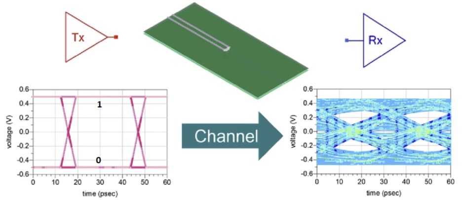
Image Credit: Sierra Circuits - Proto Express®, Understanding Signal Integrity
Signals deteriorate quickly when ground integrity fails. You'll first notice waveform distortion, where signals lose their intended shape. These issues are reduced noise margins and timing errors on oscilloscope measurements.
Ground bounce is one of the most common signal integrity problems. It happens when voltage levels at different ground reference points fluctuate because of rapid current changes through ground impedance. The low state of digital signals might bounce high enough that the system reads it as a high state. This leads to double-switching or disrupts operations.
Your prototype might work perfectly in the lab but fail in production or out in the field. Such inconsistencies often point to ground-related signal integrity issues that become more noticeable under different environmental conditions or manufacturing tolerances.
Boards with densely packed traces suffer from increased crosstalk when grounding is poor. Without enough ground references, high-frequency signals couple electromagnetically between adjacent conductors, creating unwanted interference that corrupts data. Discontinuous ground planes beneath signal paths make this problem even worse.
EMI/EMC Test Failures Linked to Ground Issues
System-level EMC failures usually tie back to grounding problems. These issues show up in specific ways during compliance testing:
- High-frequency radiation from incomplete return current paths
- Conducted emissions traveling through power and ground planes
- Excessive noise coupling into I/O lines and connectors
- Radiated emissions from signal traces acting as unintended antennas
EMC test failures often happen because of inadequate coplanar ground or missing dedicated ground planes. Multiple disconnected grounds are meant to isolate signals and prevent high-frequency components from finding low-impedance return paths. This increases radiation and may cause compliance failure.
Splits or holes in ground planes create uneven areas that increase impedance in power and ground planes. These breaks force the return current to take detours, expanding loop areas and significantly increasing inductance. High-speed traces then act like antennas that radiate electromagnetic waves, interfering with internal circuits and external devices.
Intermittent errors that point to return path problems
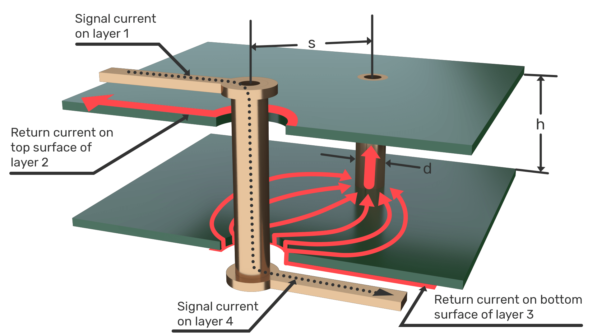
Return path issues often lead to mysterious failures that come and go. A circuit that works sometimes but not others usually points to return path problems. These issues worsen at higher frequencies where return current follows the path of least impedance instead of least resistance.
Empirical testing shows that traces crossing gaps in ground planes produce harmonics about 5 dBmV higher near the gap compared to traces over solid ground planes. These gaps allow harmonics to appear even on unpowered traces, suggesting unintended coupling.
Single-ended signals see dramatic effects from return path discontinuities on supply bounce. Return current must find new paths around discontinuities like vias, slots, or plane changes. This creates larger loop areas, increases inductance, and adds delay. High-speed busses with strict timing requirements suffer the most.
Ground loops from long signal return paths work like radiating antennas. These loops generate common-mode currents that measure 20 dB higher when traces cross gapped ground planes than continuous ones. This explains why an Ethernet port might not work until someone adds a ground jumper to provide a proper return path-even though it passed basic design rule checks.
With proper grounding, high-speed designs have the potential to work reliably in all conditions and environments. It's not just about avoiding problems; it's about building robust systems that can withstand the test of time. With the right grounding strategies, success is not just a possibility; it's a likelihood.
Stackup Planning for Optimal Return Current Flow
High-speed PCB designs need stackup planning as their foundation. This planning directly affects how return currents flow throughout the board. A well-laid-out stackup will give you short and predictable high-frequency return paths. This minimizes EMI and preserves signal integrity. Let's get into creating stack-ups that make return current flow better.
Selecting the Right Layer Count and Arrangement
Arranging signal, power, and ground layers is crucial for proper return path performance. A 4-layer PCB supporting high-speed signals can use three main configurations:
- Option 1 (Signal-Ground-Power-Signal): Most designers consider this the best choice. It allows you to route flexibly and place components on both sides.
- Option 2 (Signal-Signal-Power-Ground): You can place components on both sides but your signal routing options are limited because internal signal layers might create crosstalk.
- Option 3 (Signal-Power-Ground-Signal): This works great for high-power needs, but you can only put high-speed signals on one layer.
Designs that need more signal routing space will require 6 or 8 layers. Boards with more than 8 layers might need several plane layers for power while keeping multiple signal layers.
Here are some guidelines for boards with moderate layer counts:
- You can split power planes into multiple rails if signals don't reference that plane
- Keep power planes separate with ground planes between them
- Put fast signals between two ground planes so they don't reference split power planes
- Use surface layers mainly for fast microstrips and essential power routing
Material Considerations for High-Speed Return Paths
Your choice of materials substantially affects return path performance. High-speed digital designs need these material factors:
- Dielectric Constant (Dk): Lower Dk values let you use wider line widths with a given substrate thickness, making manufacturing more manageable. Materials must maintain stable Dk during high-speed operations to maintain consistent impedance.
- Loss Tangent (Df): Lower Df values reduce signal attenuation, especially at higher frequencies. But between power and ground plane pairs, higher Dk values with higher losses actually help power integrity by dampening resonances.
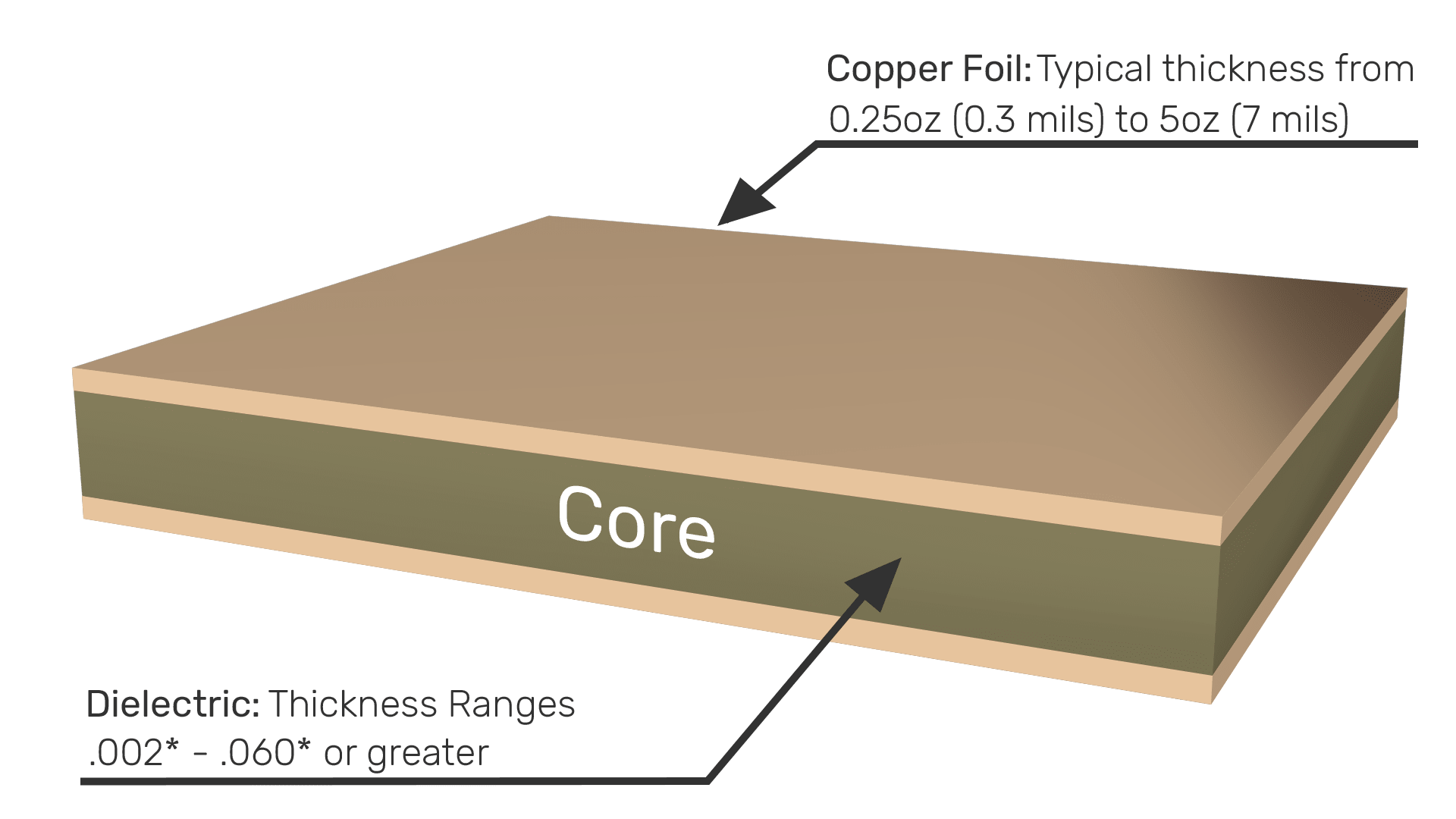
- Copper Thickness: Thicker copper means less resistance and better signal propagation through lower inductance. The downside is that it makes impedance control trickier and might need wider traces, which could increase crosstalk.
Advanced high-speed designs often use reinforced Polytetrafluoroethylene (PTFE) laminates. These offer reduced thickness (below 4 mils) without needing complex HDI processing. Embedded capacitance materials with high Dk values (from ~4 to ~10 from 100 MHz to 1 GHz) can boost power delivery between power and ground planes.
Power and Ground Plane Pairing Strategie
Clean, high-speed signals need a low-impedance power distribution network. This is achieved by correctly pairing power and ground planes. To achieve the lowest impedance for power distribution, power and ground planes should be kept as close as possible.
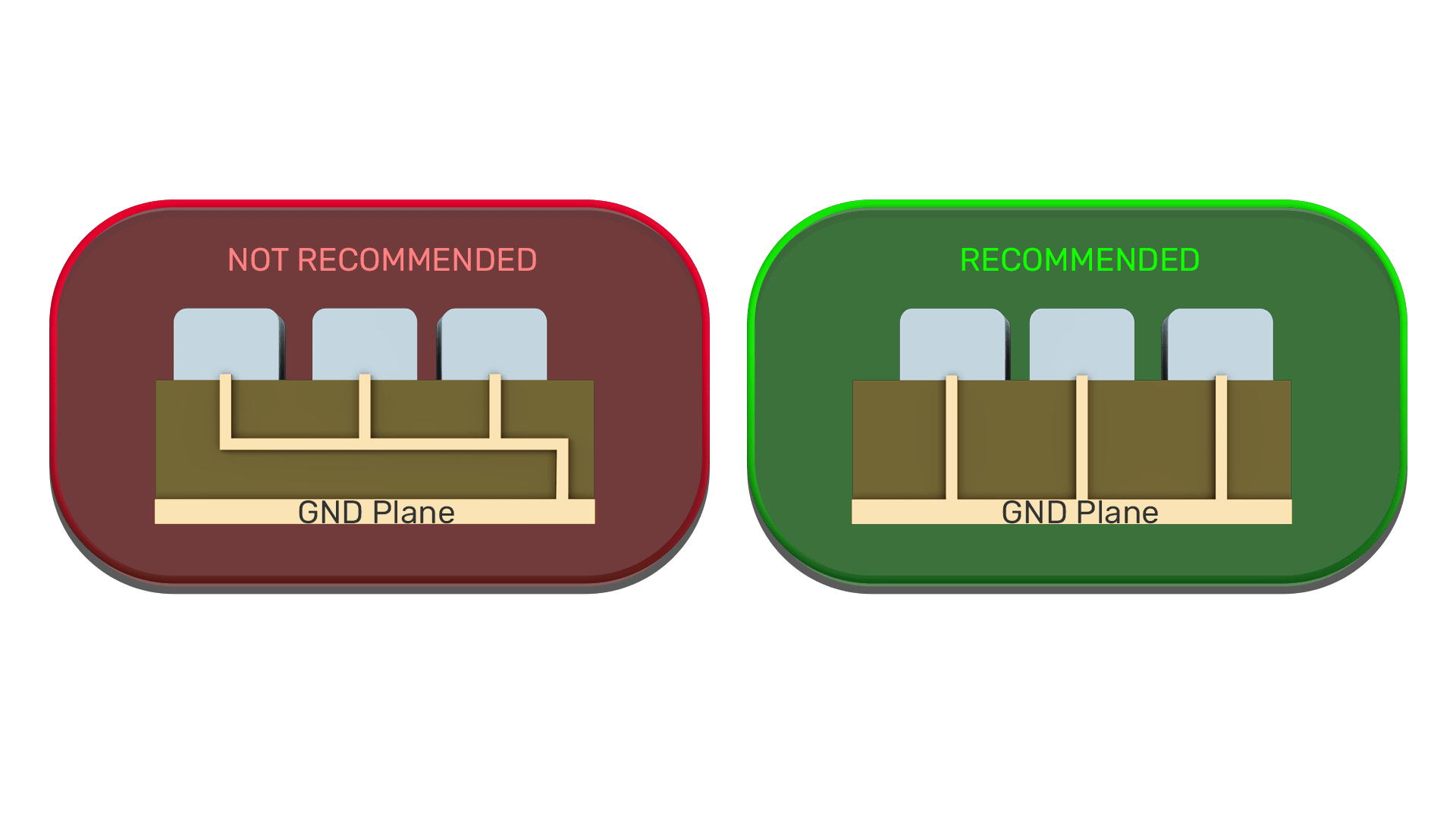
Your return paths will work best if you:
- Keep power and ground planes close together to create natural capacitance
- Put signal layers next to solid ground planes, not power planes
- Use continuous, unbroken ground planes for clear return paths
Another important aspect to keep in mind is that split ground planes create significant problems for return currents. Traces crossing a ground plane gap show harmonics about 5 dBmV (deciBels relative to 1 milliVolt) higher near the gap compared to traces over solid ground. These discontinuities create return paths with high loop inductance, leading to more radiation and potential EMC compliance issues.
Mixed-signal designs don't really need separate analog and digital grounds. This separation often causes more problems than it solves. A better approach uses a single, continuous ground plane with careful signal routing. This prevents digital return currents from flowing through analog sections.
A good layer stack-up means you'll need fewer decoupling capacitors. For example, a four-layer PCB works great when you use the two bottom layers as ground and power planes. Put signals on top and add another ground plane right underneath. This creates a very low-impedance power distribution network.
In Part 1, we explored how return current paths shape signal integrity and why grounding strategy is the backbone of high-speed PCB design. Now, let's dive into how thoughtful component placement and routing decisions help maintain those critical return paths and prevent signal degradation in Part 2 of this series.