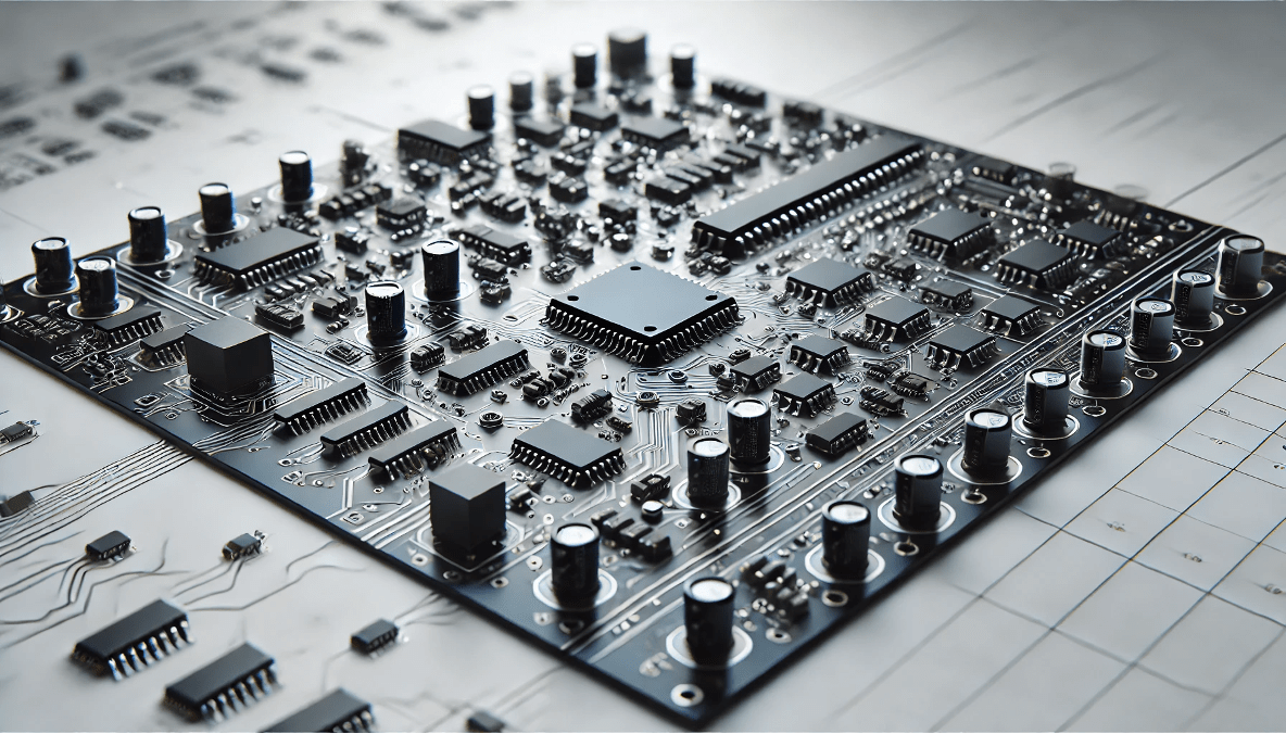
When to Use Copper Pour and Via Stitching In PCB Design
In the intricate world of printed circuit board (PCB) design, two techniques stand out for their significant impact on performance, reliability, and electromagnetic compatibility: polygon copper pours and via stitching. While serving different primary functions, these methodologies can complement each other to create robust circuit designs that meet the demanding requirements of modern electronic devices. Understanding the strategic implementation of copper pours and via stitching can dramatically improve your design outcomes, whether you're working on high-frequency applications, power-intensive circuits, or designs requiring strict electromagnetic compatibility.
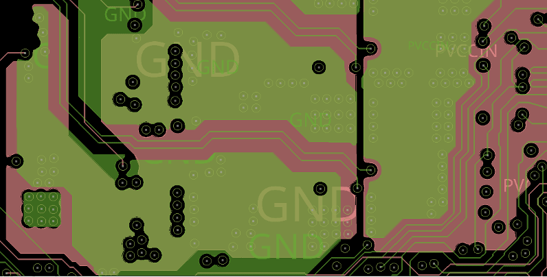
Understanding Polygon Copper Pours
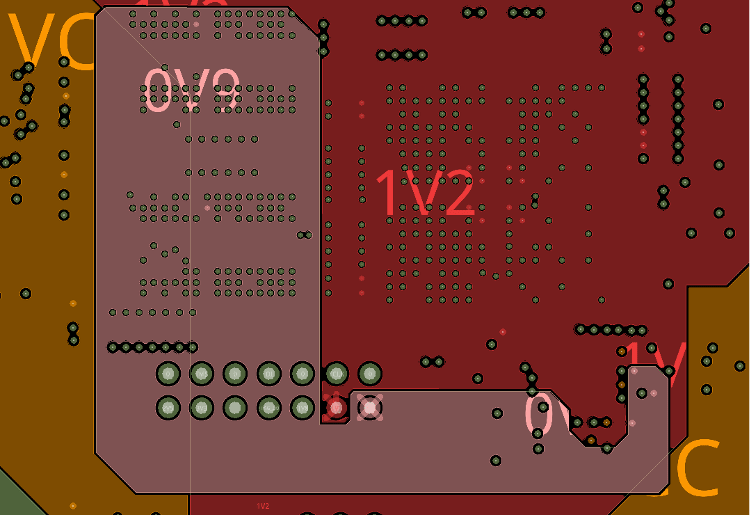
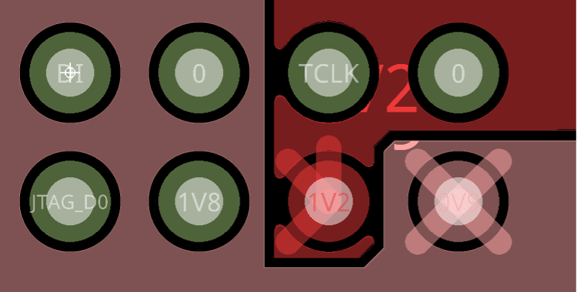
Polygon copper pours represent areas of copper that extend beyond traditional traces on a PCB. These expansive metal regions serve multiple crucial functions in circuit design. Unlike standard traces that connect specific components, copper pours create large conductive areas that can be assigned to particular nets, most commonly ground or power.
Definition and Basic Functionality
A polygon copper pour, sometimes called an area fill or copper region, is a technique for creating extended areas of copper on PCB layers. These pours can be shaped as needed-rectangular, irregular, or following the board's outline, and are typically connected to specific nets in the circuit. Modern PCB design software allows for the creation of these regions with precise control over their boundaries, clearances, and connections to other elements.
When implemented, these copper areas maintain proper clearance from traces and components belonging to different nets, adhering to the board's design rules. The pour can connect directly to pads and vias of the same net, creating reliable electrical connections throughout the design.
Applications and Benefits
Copper pours serve numerous essential functions in PCB design:
- Ground and Power Distribution: Large copper areas provide low-impedance paths for ground returns and power distribution, reducing voltage drops.
- Thermal Management: Expanded copper regions efficiently dissipate heat from components, which is particularly beneficial for power devices that generate significant thermal energy during operation.
- EMI Reduction: Continuous ground planes created by copper pours minimize electromagnetic interference by providing shorter signal return paths.
- Signal Integrity: Copper pours help preserve signal quality by maintaining consistent reference planes for signals, especially in high-frequency applications.
- Current Handling: For circuits requiring high current capacity, copper pours offer substantially more metal cross-section than standard traces, reducing resistance and associated heating.
When to use Copper Pours?
When implementing polygon copper pours in your designs, several factors warrant careful consideration:
- Thermal Relief Connections: When connecting components to large copper areas, thermal relief connections (spoke-like connections) are typically used to facilitate soldering by preventing the copper pour from acting as a heat sink during assembly.
- Isolation Requirements: Sometimes, you may need to create cutouts or splits in copper pours to isolate different circuit sections or prevent unwanted current paths.
- Pour Order: In complex designs with multiple overlapping pours, the order of pour creation can affect the final result, as later pours respect clearances from earlier ones.
- Hatched vs. Solid Fills: Depending on your application, you might choose between solid copper fills or hatched patterns, which use less copper but maintain electrical connectivity.
Via Stitching Explained
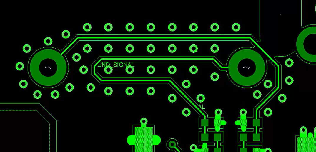
Via stitching represents a strategic approach to PCB design where multiple vias are placed in a methodical pattern to connect copper areas across different layers. This technique enhances electrical performance, improves thermal characteristics, and addresses electromagnetic compatibility concerns.
Definition and Core Principles
Via stitching involves placing numerous vias, typically in grid-like arrangements, to connect copper areas across multiple PCB layers. These vias create vertical electrical connections through the board's structure, effectively binding together copper regions that would otherwise remain isolated on their respective layers.
The vias used in stitching are usually smaller than those used for component connections and are placed at regular intervals determined by the design's specific requirements. These vias' spacing, size, and pattern significantly impact their effectiveness for different applications.
Primary Applications
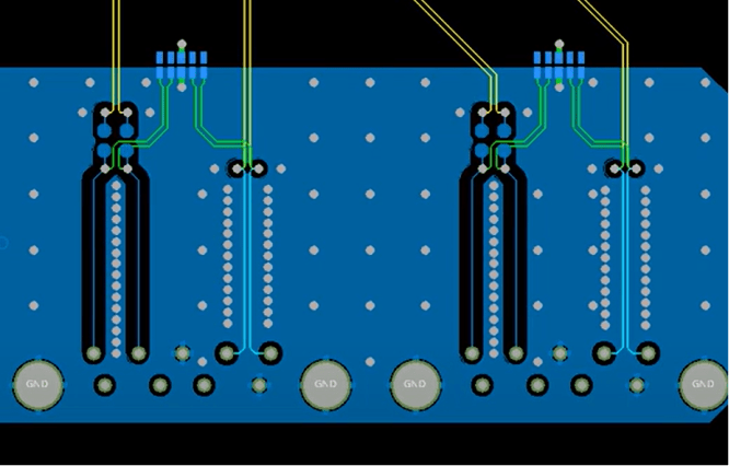
Via stitching serves several critical functions in PCB design:
- Ground Plane Connectivity: Connecting ground planes across multiple layers, via stitching creates a robust three-dimensional ground structure that minimizes ground impedance.
- EMI Shielding: Properly spaced via stitching around sensitive circuits or along board edges forms an electromagnetic barrier that contains radiation within the board or blocks external interference.
- Thermal Management: Stitching vias helps transfer heat between layers, improving overall thermal performance by creating multiple paths for heat dissipation.
- Signal Integrity: For high-speed signals, via stitching near signal transitions helps maintain consistent return paths, reducing signal degradation.
- Mechanical Reinforcement: Stitching can enhance the board's structural integrity in areas subject to mechanical stress, such as connector mounting points.
Implementation Strategies
Effective via stitching implementation requires consideration of several key factors:
- Via Spacing: The distance between stitching vias determines their effectiveness at containing electromagnetic fields. For EMI shielding, spacing should typically be less than one-tenth of the wavelength of the highest frequency of concern.
- Via Size and Type: The diameter and construction of stitching vias affect their electrical and thermal characteristics. Smaller vias may be used in dense designs, while larger ones offer better current-carrying capacity.
- Pattern Selection: Different arrangements-grid patterns, perimeter rings, or targeted placements near sensitive components-serve different purposes and should be selected based on specific design requirements.
- Layer Transitions: For high-speed signals, carefully designed via stitching near layer transitions helps maintain signal integrity by providing well-defined return paths.
When to Use Polygon Pours and Via Stitching
When working with copper pours and via stitching, it's essential to recognize each technique's unique strengths and limitations. In high-speed PCB design, these aren't just layout preferences; they're strategic tools that directly impact signal integrity, EMI performance, and thermal management. Understanding how to leverage polygon copper pours, via stitching, or a combination of both depends on the specific needs of your design. Factors like return path continuity, layer stackup, frequency, and even manufacturability play a role.
So, let's dive in and look at some scenarios where these techniques are commonly used.
Polygon copper pours generally prove most beneficial in these situations:
- Power Distribution Networks: When designing circuits with significant power requirements, copper pours provide the low-resistance paths necessary for efficient power delivery.
- Single-Layer Grounding: For simpler designs where ground connections primarily exist on one layer, a copper pour offers a practical solution without the complexity of via stitching.
- Heat Dissipation Requirements: Components generating substantial heat benefit from adjacent copper pours that help spread thermal energy across larger areas.
- Cost-Sensitive Applications: Since copper pours don't require additional drilling operations, they can be more economical than extensive via stitching in cost-constrained projects.
Via stitching becomes particularly valuable in these contexts:
- High-Frequency Designs: Circuits operating at high frequencies benefit from the reduced loop areas and controlled impedance that well-implemented via stitching provides.
- Multi-Layer Grounding: Complex boards with ground planes on multiple layers require via stitching to create a unified, low-impedance ground structure.
- EMI-Sensitive Applications: Products that must meet stringent electromagnetic compatibility requirements often rely on via stitching to contain radiation and reduce susceptibility to external interference.
- Signal Integrity Challenges: Designs with critical high-speed signals benefit from via stitching that maintains consistent return paths across layer transitions.
Utilizing Both Techniques for Optimal Results
Integrating copper pours, via stitching or a combination of both isn't just a best practice; it's a powerful design strategy when applied with intention. Rather than treating them as isolated techniques, combining them thoughtfully can address multiple design challenges.
When implementing, consider these effective strategies:
- Ground Plane Enhancement: Create substantial ground copper pours on multiple layers, then connect them with methodically placed stitching vias to form a comprehensive three-dimensional ground structure.
- Thermal Management Systems: Implement copper pours near heat-generating components, then add stitching vias to transfer heat to internal or opposite-side copper layers for improved dissipation.
- EMI Containment Structures: Design copper pour "fences" around sensitive circuits or along board edges, reinforced with closely spaced stitching vias to create practical electromagnetic barriers.
- Power Distribution Networks: For high-current applications, combine wide copper pours with multiple parallel stitching vias to create low-impedance power delivery paths across layers.
By strategically integrating these techniques, you can elevate your PCB designs beyond the basics. The key is to align their strengths with your design needs. When done right, they don't just solve problems; they unlock performance.
Key Takeaways for PCB Design
Polygon copper pours and via stitching represent two fundamental techniques in the PCB designer's toolkit, each offering distinct advantages for specific applications. While copper pours excel at creating expansive conductive areas on individual layers, via stitching provides crucial vertical connections that unify copper regions across multiple layers.
The most effective PCB designs often leverage both approaches, strategically implementing copper pours where expanded conductive areas are needed and adding via stitching where vertical connectivity enhances performance. By understanding each technique's principles, applications, and implementation considerations, you can make informed decisions that optimize their circuits for reliability, performance, and electromagnetic compatibility.
As electronic devices continue to advance, operating at higher frequencies, consuming more power, and requiring greater integration, mastery of these fundamental PCB design techniques becomes increasingly valuable. Whether designing simple two-layer boards or complex multi-layer systems, the thoughtful application of polygon copper pours and via stitching will remain essential to creating successful PCB designs.