An Introduction to Microvias in PCB Design
Microvias are a key feature in modern PCB design, especially for high-density interconnect (HDI) technology. These tiny, laser-drilled vias enable compact, high-speed designs by connecting copper traces between PCB layers. In this blog, we'll explore the types of vias, the advantages of microvias, and their role in enhancing signal integrity, power integrity, and thermal management.
What are Vias in PCB Design?
Vias, or vertical interconnect accesses, are conductive pathways that electrically and mechanically connect copper traces between different layers of a printed circuit board. In essence, a via is a plated hole, filled or left open, that bridges one or more copper layers, enabling signals, power, or ground connections to traverse the layered PCB stack-up. Vias come in several forms:
- Through-hole vias: Extend from the top to the bottom of the PCB
- Blind vias: Start from an outer layer and terminate at an internal layer
- Buried vias: Exist entirely between inner layers and are invisible from the surface
Traditional via structures are created with mechanical drilling followed by platting. While this method is robust and widely used, it can introduce the following challenges in high-density PCB layouts:
- Space consumption: Large diameters take up valuable board real estate, complicating routing in compact designs.
- Signal integrity issues: Via barrels can cause parasitic capacitance and inductance, leading to reflections and impedance discontinuities.
- Mechanical reliability: Deeper vias with high aspect ratios risk plating defects like voids or cracks.
Why Microvias Are Essential for HDI PCB Design
HDI technology addresses these challenges with microvias: small, shallow holes (less than 0.25 mm deep) created using laser drilling. Microvias offer several advantages:
- Compact size: Ideal for high-speed, fine-pitch designs.
- Improved signal integrity: Reduced parasitic effects compared to traditional vias.
- Enhanced reliability: Lower aspect ratios improve plating quality
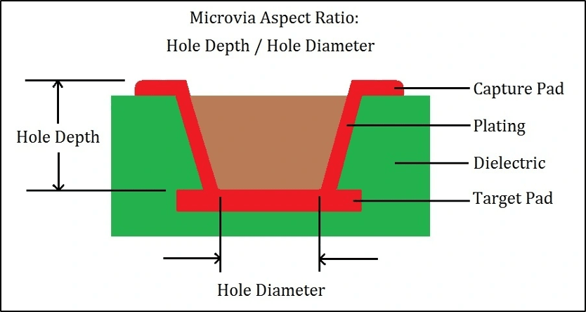
Figure 1: Microvia diagram showing depth and diameter, microvia aspect ratios range 0.6:1 to 1:1 with diameters from 50 up to 250 µm. Source: Cadence
Microvia Configurations
High-speed digital (HSD) designs push PCB density to the limits, with components such as ASICs (Application-Specific Integrated Circuits) and FPGAs (Field-Programmable Gate Arrays), often packaged in CSP, BGA (Ball Grid Array), or µBGA formats that exceed 1,000 pins. This demands careful fan-out planning to route I/Os from central ball patterns to deeper layers, while maintaining uniformity and minimum line widths.
As shown in Figure 2, microvias can be stacked or staggered in configurations such as 3+N+3 or greater:
- Stacked Microvias: Require internal vias to be filled and capped
- Staggered Microvias: Provide a conductive path without a microvia fill or copper capping
The placement of vias and the distribution of blind/buried holes are critical when fanning out from a fine-pitch, high-pin-count integrated circuit (IC), because an asymmetric stack can cause uneven pressure during fabrication and result in board warpage.
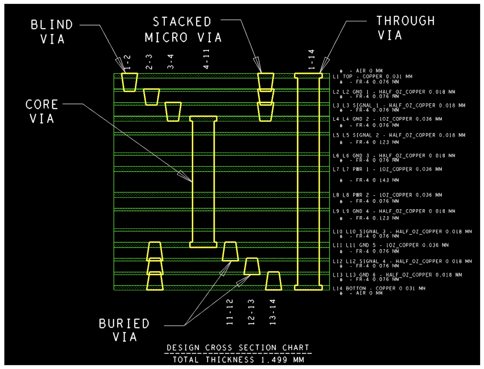
Figure 2: A 14-layer 3+N+3 board showing stacked and staggered microvia configurations. Source: Cadence
Enhancing Signal Integrity with Microvias
HSD designs generate RF energy that can cause signal integrity issues, including harmonics that can extend into the millimeter-wave range. Any signal path branching out is a potential stub, which can resonate within the HSD bandwidth and cause destructive interference and signal power dips at resonant frequencies. If this dip occurs in areas of significant signal energy, it can distort waveforms and increase the bit error rate (BER). Therefore, short via lengths are crucial.
This is where blind and buried microvias excel, offering electrical advantages over traditional through-hole vias and lower self-inductance. However, their aspect ratios require thin substrates (around 60 µm) on HDI outer layers. Under these conditions, maintaining 50-ohm impedance requires impractically small trace widths, as impedance depends on dielectric thickness, dielectric constant, trace width, and spacing. Routing transmission lines on internal layers allows for wider traces, which reduces both self-loop and overall transmission line inductance and improves signal integrity.
Improving Power Integrity with Microvia VIPs
Via-in-pad (VIP) microvias connect IC landing pads directly to internal layers, improving power integrity by:
- Reducing parasitic inductance: Shorter current loops enhance decoupling performance.
- Improving transient response: Capacitors can respond more effectively to current demands. (Figure 3)
Compared to standard through-hole VIPs, microvia VIPs can reduce inductance and capacitance by up to 90%, significantly enhancing power integrity behavior.
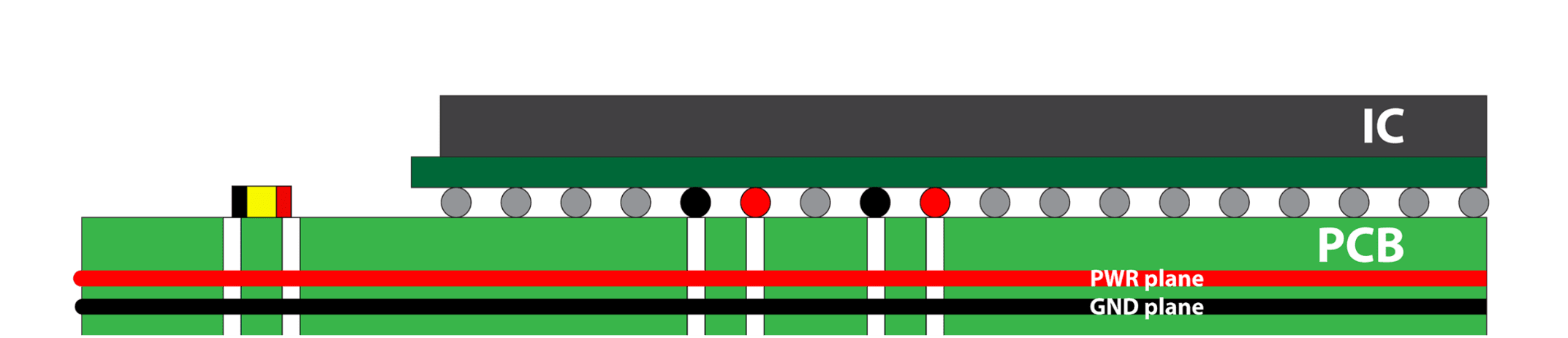
Figure 3: Illustration of decap mounting on PCB using VIP to the power and ground planes.
Addressing Soldering Challenges with Microvia VIPs
Microvia VIPs can cause soldering issues if they are not properly plugged, as solder can wick down through the open via holes by capillary action, leaving less solder to secure the component. Whether the via is on or near the landing pad, preventing it from drawing away solder intended for the pad is crucial to avoid opens, shorts, tombstoning, or interference with nearby components.
Thermal Management for Microvias
In HDI designs, thermal management is critical due to tightly packed components and mismatched coefficients of thermal expansion (CTEs).. This thermal stress can cause mechanical problems such as microvia barrier cracking and delamination, as well as electrical failures.
The first line of defense is to channel as much heat away from hotspots as possible, reducing the risk of thermal-related failures. In many designs, microvias serve this role, providing a direct thermal pathway from the large ground pin, often located at the center of quad-flat-package (QFP) devices, into the inner layers of the PCB, where heat can be dissipated more efficiently.
Common Microvia Failures and How to Prevent Them
Microvia failures often result from z-axis thermal expansion, where the differing CTEs of the dielectric and copper become a serious concern. Secondary causes include artwork inconsistencies and fabrication issues, such as plating defects or other process variations.
Common failures include:
- Dislocation from the target pad
- Barrel or corner cracks
- Misregistration
- Target pad pull out
- Copper voids or cap separation
Overcoming HDI Complexities with the Right Tools
The Allegro X System Design Platform and the OrCAD X Platform offer robust microvia support, covering stacked and staggered configurations, within its HDI routing tools. In the Padstack Editor, designers can select microvias and set the clearance matrix (Figure 4), defining spacing rules for microvia-to-microvia, microvia-to-core via [blind and buried (BB)], and microvia-to-through-hole.
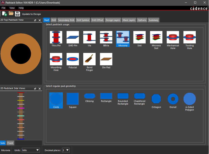
Figure 4: The Padstack Editor in Cadence can be used to create a microvia. Source: Cadence
The Constraint Manager defines rules for same-net spacing, independent of net-to-net spacing. The Cross-Section Editor in Allegro X/OrCAD X allows detailed stackup design, including material properties, which are critical for mitigating z-axis thermal expansion. Allegro X/OrCAD X's DFM checks help ensure microvias meet manufacturing tolerances and maintain reliability. Thermal analysis tools can also accurately identify hotspots and evaluate heat distribution across the HDI board, providing engineers with a complete view of thermal performance.
Final Thoughts on Microvias in Modern PCB Design
Microvias are foundational to today's HDI designs, enabling dense fan-out, cleaner signal paths, tighter power loops, and more effective thermal escape routes; all within increasingly compact form factors. By leveraging blind, buried, and via-in-pad structures, designers can minimize parasitics, reduce BER risk, improve decoupling performance, and enhance overall reliability. Success, however, depends on getting the details right: balanced stackups, appropriate aspect ratios, correct via fill/plug strategies, and rigorous DFM and thermal checks to mitigate z-axis expansion and plating defects.
With robust design rule control, accurate stackup definition, and integrated analysis, tools like Allegro X and OrCAD X streamline HDI workflows and help teams implement microvias with confidence. As pin counts rise and edge rates climb, microvias aren't just a convenience; they're a necessity for performance, reliability, and manufacturability in next-generation electronics.