Flex Circuit Design Practices For Manufacturing and Assembly
Flexible Printed Circuit boards or FPC's allow circuits to mold themselves to geometry as varied as can be imagined. That freedom to shape-shift into different form factors comes with an equal amount of responsibility. Our friends on the MCAD end of the CAD cave may need our ECAD guidance when it comes to enduring reliability.
Even the simplest flex in the form of a bespoke cable deserves to be put to the test. The first iteration might call for something more flexible than we can accommodate. We are the final gatekeepers of quality when it comes to the world of FPCs and FPCAs.
Mocking Up a Flex Circuit To Ensure Correct Connectivity
I've heard that there are ways of planning a flex in collaboration between MCAD and ECAD using just the software; no idea how that would work. I used "paper dolls". These are ordinary pieces of paper that are cut to shape and used with mock-up printed circuit boards. We basically verify that a flex will have the correct orientation through all of the bends and folds of its final shape.
Working through the 3D landscape helps verify that the connector is on the right side of the flex and that pin-one is in the correct corner when it comes to final assembly. We also want to know that pin-one means the same thing from one connector to another within the system of printed circuit boards. A 3D printer is great for making blanks of the rigid board(s) as a starting place for a flex circuit study. If you have a Mechanical Engineer who can work with you in the virtual world, so much the better.
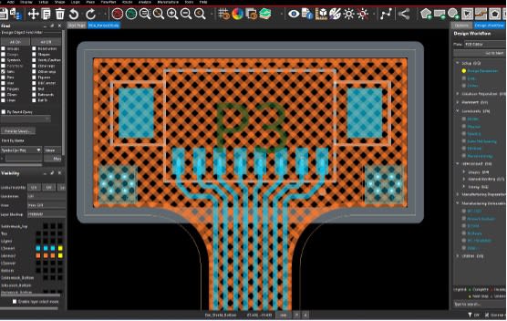
Figure 1. The tail end of a flex is one place where a number of design choices come into play. Here, we have the flex outline plus 1.27 mm thickness, shown in grey. The traces pass through the "grey area" perpendicular to the line. It represents the transition from the stiffener to the flexible area. Image Credit: Author
In some regards, a flex circuit is more mechanical than electrical. A one-layer flex is likely to have all of the connections made with no cross-overs. The routing bus has the same pin-out at either end so we connect the dots. That kind of routing is about 5-10% of the effort that goes into an FPC.
The Mechanical Outline: A Series of Contradictions
One aspect of FPC design is that some areas have to be rigid. The result is that we have to create and curate a collection of FPC stack-ups for each region or zone of the FPCA. By default, the flexible zones use copper clad polyimide material for construction. The outer layers become inner layers with the addition of coverlay.
The material for the coverlay is also polyimide but without any metal cladding. An adhesive is applied to join the two dielectric layers, forming a copper sandwich. That is the perfect balance to strike for good flexibility, metal between two layers of film. The flexible areas may also have another layer that mitigates signal integrity issues. The EMI film needs to touch down on some grounded metal in strategic locations. We create holes in the coverlay and selectively pour solid copper for each grounding location.
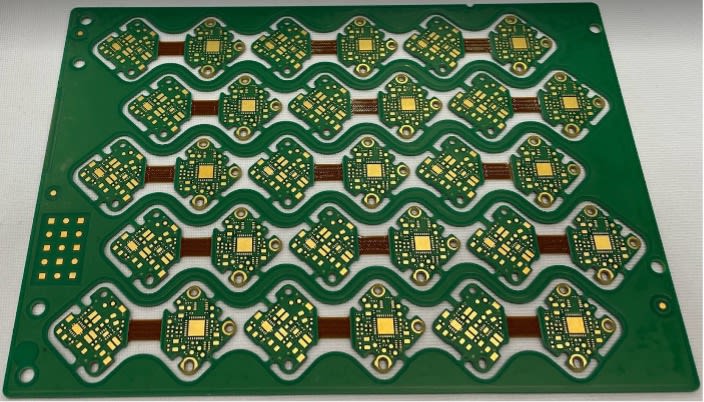
Figure 2. This is an assembly sub-panel for a simple rigid/flex design. The fabrication panel would have this sub-panel repeated a number of times. Following SMT soldering and test, depaneling is done by cutting the four break-off tabs on each FPCA. Each tab is slightly recessed into the edge of the board outline so that nothing protrudes after depanelization. Image Credit: Author
The edge of the stiffener would fall inside the flex outline if it was made of FR4 or steel. If the stiffener was made of polyimide, then the outline and the stiffener would be the same size as the flex outline. All of the layers would be cut out at the same time in that case.
Placement is Often Predetermined By The Outline Drawing
Placement of the connectors is usually a system level affair. The mechanical engineer will start with the number of traces and spaces and use that data to get the minimum width of the flex. I've found myself in this situation.
It was important to be able to use the "hug" option to keep every trace as close as allowable so that there's just enough room for the last trace or row of GND vias - if that's part of the plan. The spacing constraints will be set to the minimum gap while "neck mode" may be used in the most compact areas for narrow traces.
Routing Traces When They Are Hemmed In
One of the hallmarks of flex circuit routing is the use of arcing traces to follow radiused outlines. You would draw one trace along the edge of the route keep-in through the radial bend in the flex outline. Then, with a very fine grid, you would slide the arc against the route keep-in until it cannot get any closer. Every trace that uses that corner will be packed in using the hug command to route or slide as necessary so that the final trace has sufficient room.
Another thing about FPC design is that rigid boards have been behind flexes in terms of minimum line width and spacing. A 50 micron trace is old news on an FPC. Once gathered from the connector, the traces of a flex circuit tend to stay in their lane. There will be cases where two routing schemes are not one-to-one in terms of pin-out.
In that case some additional stiffened area may be required to untangle the traces at one or both ends. In figure 3, we see the coverlay in green up onto the stiffened zone. The coverlay is topped with an EMI shielding material that touches down on the two ground pads flanking the connector.
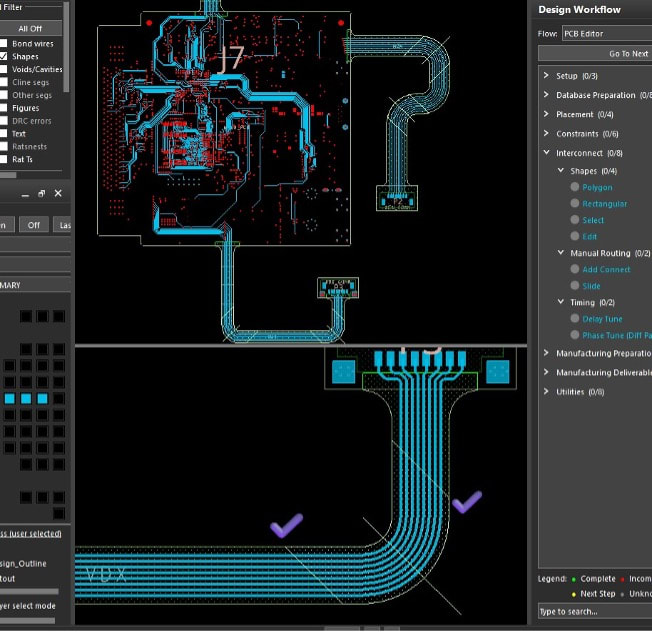
Figure 3 Demonstrating the split screen feature, the checkmarks are there to highlight a "bend group". The line and any associated shapes, including via keep-out areas, are reusable once the group is created. In this case, the original and three copies. Image Credit: Author
Bend regions are a special case. The flexing puts stress on a via which can cause it to fail. Meanwhile, the via also inhibits bending of the part we need to bend so consider the entire bend region to be a via-free area.
Knowing this, I shy away from adding vias in the vicinity of the bend region. I've been in the design review where they ask, "Do you have to put vias so close to the bend regions?" Answer: Not if I add a few mm of via keep-out to each of the shapes. "How much is enough?" A few millimeters.
Notice Figure 3 has the purple check icons to help locate the beginning and end of the bend region. The yellow line across the apex of the turn is the actual bend line. The radius of the bend would be specified in the fab notes. It's on us to ensure that the final bend radii are within the process window while meeting the form factor. It may require pre-bending.
While I'm at it, I would go to the mechanical engineer and ask about bending the flex along the straight sections. Also widening the whole channel so that some ground strips could be added along the edges would be an improvement. At minimum, a room for a sacrificial tear-stop trace along the inside of the bends would help me sleep at night.
One last note about the bend regions is that we like to keep the copper flowing straight through the bend area. This is where we're concerned about the copper lifting from the dielectric material. Lifting pads is another thing with flex circuits. It used to be popular to add a couple of spurs to the pad. These stubs will tuck under the soldermask and/or coverlay to help anchor the pad to the dielectric material.
Calling Out Start and Finish Copper Weights
In addition to the polyimide base material, FPC designers also call out the copper in terms of starting thickness and final thickness after any plate-up. This additive way to parse the copper thickness is particular to flex circuits. We normally focus on finished copper weight.
Rolled Annealed (RA) copper is popular for flexes although it isn't necessarily required if the circuit is only flexed during installation. So we would specify RA copper for anything that flexes during service; common for robotics. Any dynamic flexing areas would entail the minimum use of copper consistent with the mission requirements.
Copper and dielectric callouts are only the beginning. Coverlay and stiffeners are both added on with different types of adhesive. EMI film is sometimes used when there are signal integrity concerns with the circuits traversing the flexible area.
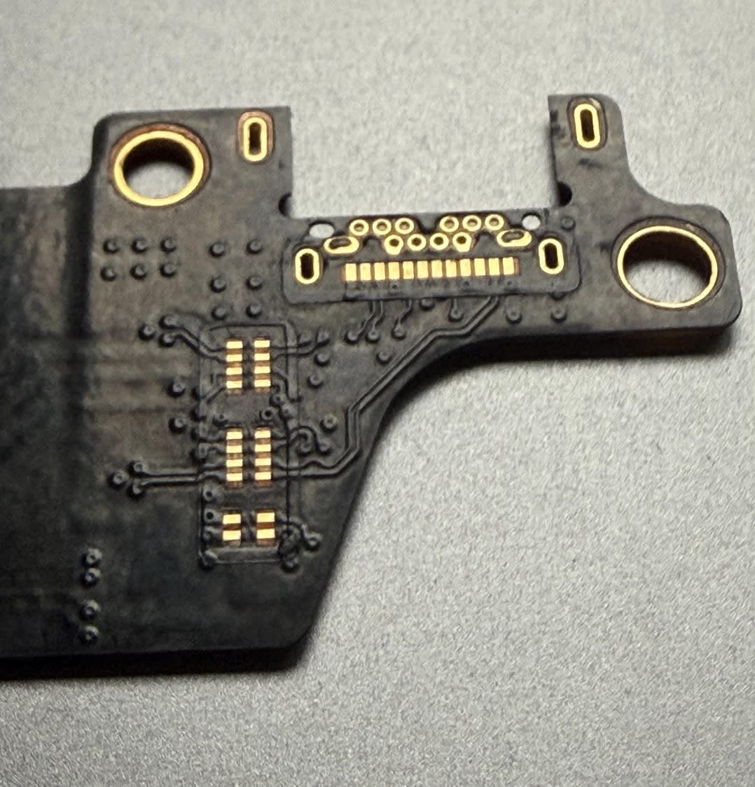
Figure 4. This USB type C connector shows some of the challenges we face for the sake of miniaturiaztion. Note the non plated hole and slot in close proximity to the through-hole pads. Some data sheet tolerances can not be achieved on an FPC. We get stuck between the part vendor and the factory. Image Credit: Author
I've never included layers for adhesive but the silkscreen, soldermask, coverlay and stiffeners should have their own artwork layers. If we were going to apply the glue selectively and leave certain bend regions as loose leaf areas, that would be cause to create specific artwork for the adhesive. Separating layers of material reduces stress when pre-forming the flex around a mandrel.
My advice on silkscreen is to keep it away from the components. The DFM reports seem to fixate on that issue. It's enough to make you want to generate specific footprints for flex circuits that go one step beyond IPC class 3 designs.
Flex circuits can be a good diversion from the normal boards. There is more interaction with the mechanical team. The routing is generally simple although the FPC universe has been doing finer lines than their rigid counterparts for quite some time. The stack-up is really a number of different substacks.
Even with all of that, there is a certain looseness with flex circuits. They're more like a hand built craft than a factory precision piece. It's a world of different materials and techniques. We would not have the sleek form factors for our electronic devices without the use of flex circuits. Robots would be harder to build without FPC's. Every designer should be able to adapt to the quirky nature of flexes.