Interconnect Technology for Chiplets
The month of August 2025 moved the Universal Chiplet Interconnect Express standard forward to revision 3. This follows revision 2 by exactly a year. The first selling point of revision 3 is higher data rates, double that of the previous version. If that sounds like another standard, PCIe, then chalk it up to UCIe using PCIe as a template along with the Compute Express Link (CXL) to build the UCIe ecosystem. It remains adaptable and scalable according to needs.
The founding members make up some of the titans of their respective industries. You've heard of them and likely others who have signed up to support version 3. It's more than the bandwidth. The sideband channel has been upgraded so that:
- "Priority sideband packets allow deterministic, low-latency signaling for time-sensitive system events" An important background command can be expedited to keep things running efficiently.
- "Fast throttle and emergency shutdown mechanisms provide immediate system-wide notifications via open-drain I/O" Dovetails with the bullet point above where the system can manage thermal shutdown issues.
- "Support for continuous transmission protocols through mappings, enabling uninterrupted data flow in Raw Mode …" This feature enables ADCs to get the uninterrupted feedrate required for seamless operation.
- Backwards compatible with existing UCIe protocols.
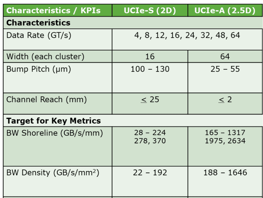
These are among several other bullet points that separate version 2 from version 3. The spec is broken down into two general connectivity schemes; UCIe-S (Standard Package, 2D) and UCIe-A (Advanced Package, 2.5D).

Figure 1. The bump pitch for either technology seems ridiculous for a PCB Designer. Additive technology can do some fascinating stuff. Image Credit: Dr. Debendra Das Sharma - (UCIe Chairman); V3 press release, snipped from a larger table.
The idea of "heterogeneous integration" is not so new. My jumping-in point was around the turn of the century. Big Bear Networks was a startup doing all sorts of innovative things in the optical space around OC192 and OC768 specifications. This is where 10GB/s and 40GB/s come into play. We had a Multi-Chip-Module (MCM) with two chips and a row of tiny passive components. The first chip consumed a single pair of transmission lines for 40G and would output four lanes of 10G. It had the usual complement of control lines and a PLL (Phase Locked Loop) circuit.
The other chip drank straight from the four 10G feeds and provided four lanes at 2.5GB/s each for a total of 16 differential pairs over copper from a single fiber. Around the data center, things will be an order of magnitude more intense. The difference between board and substrate materials (& processes) starts to blur. This multi-chip-module used LTCC, Low Temperature, Co-fired Ceramic material for the dielectric.
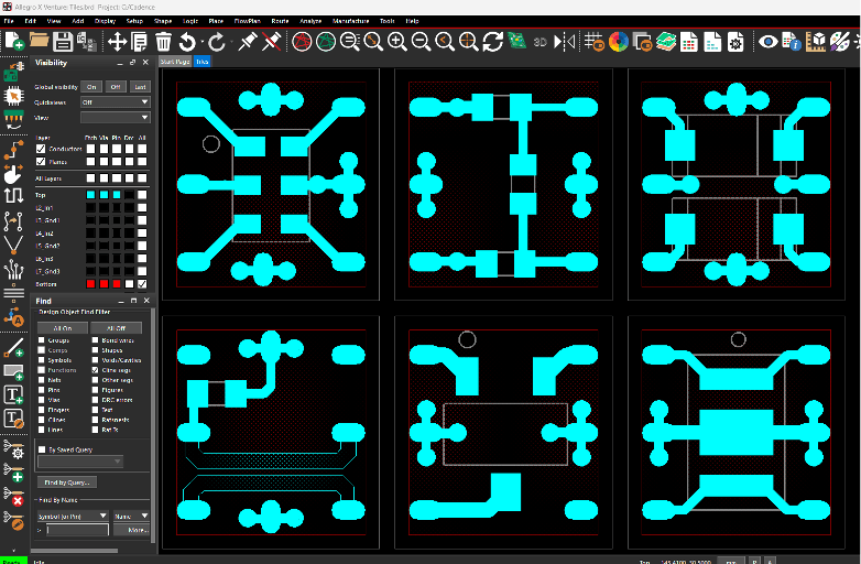
Another project used thin film. It was kind of like building a jigsaw puzzle one tiny circuit at a time. I was creating these little squares each with a primitive circuit that fanned out to wirebond pads. The small pieces were attached individually on a substrate then components and wirebonds were added to make the circuit assembly complete.

Figure 2. An assortment of primitive circuits were cobbled together and connected with wirebonding. There were size limits for the thin film technology so only the smallest packages were supported. Chiplets use flip-chip technology whereas this experiment is set up for wirebond connections using packaged electronics. Image Credit: Author.
I had no idea what we were doing until I saw the mosaic of little circuits where my job was to create a wirebond diagram. After spending a summer as a tile setter's helper, I looked at the different circuit patterns as tiles. The most popular tile had a resistor footprint plus a test point along with the two wirebond pads. Anyway, the EE did the "tile setting" with the schematic in his head at that point.
Looking at many different chiplet configurations online, the substrate layout mirrors what we would do on a PCB except with each of those chiplets in its own package. To that end, priority for routing goes to the memory cache while the quiet zone is occupied by wireless technology. It comes down to small-scale board design.
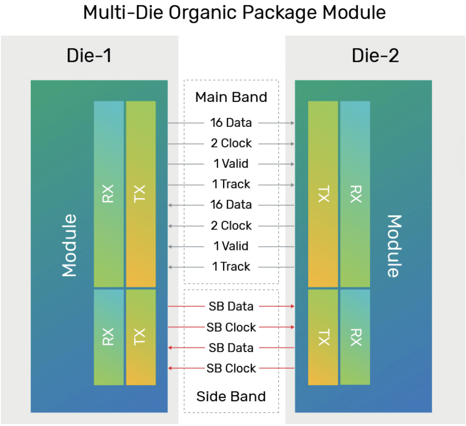
The edges of a chiplet are known as a beachfront. It's where the interaction is defined by the spec. Standard density yields 16 I/O pins while the advanced density uses 64 I/O pins with the same length of beachfront. The miracle is in the interposers.

Figure 3. The UCIe interconnect diagram showing the Main Band and Side Band connections between two chiplets with "Standard" organic substrate material. Using "Advanced" material enables 64 data I/O lines rather than the 16 for organic. Image Credit: Cadence
There are a few main players in the interposer game. TSMC with their "CoWoS" (Chip on Wafer on Substrate) family and Samsung with the "Cube" series seem to have the lion's share of the pie. Intel also created a standard which they share. There are a couple of standards for optical gear as well. They all operate in their specific ways while underpinned by the UCIe standard.
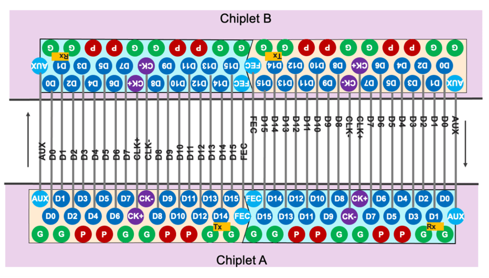
Another standard is called Bunch of Wires. I like the transparency. It is strictly a PHY specification that could lean into the UCIe standard for the die-to-die adapter and protocol layers.

Figure 4. The minimalist version of Bunch Of Wires implementation using a "full slice". The term "wires" actually refers to traces on the interposer. This could also be cut down to 8 lanes on each bunch for a half slice. Of course, it can be scaled up as well. We currently have BoW-32, -64, -128, -256, -384 or BoW-512 for increased throughput. Image Credit: Open Compute .org
Chiplets are pushing substrate design to a whole different level beyond the SOC (System on Chip). There are so many more options beyond the monolithic silicon die. Challenges remain for qualifying a mix of various chiplets. There are thermal and signal integrity concerns where the SIP (System in Package) designer has to contend with a diverse chipset under the lid of a single package. The extra freedom can be a blessing or a curse.
Whether the device will use organic material or a silicon interposer will be the dividing line between standard and advanced package solutions. Just as in PCB Design, the location of each circuit block has an oversized impact on the overall design outcome for the SIP.
I'll leave this conclusion from the standards committee. "UCIe 3.0 represents a transformative advancement in chiplet interconnect technology, addressing the critical needs of modern computing applications. By doubling data rates, supporting continuous transmission protocols, optimizing power savings, and enhancing manageability, UCIe 3.0 sets a new standard for efficient, scalable, and reliable chiplet integration."