Architecting HDI for Ultra-Fine-Pitch Chiplets, AI Accelerators, and Fan-Out Packaging on Boards
The semiconductor industry's trajectory toward chiplet-based architectures, high-bandwidth memory (HBM) integration, and advanced fan-out packaging is reshaping what PCB designers must accomplish beneath these devices. When a single AI accelerator module presents thousands of connections at 0.35mm pitch or finer, conventional HDI approaches strain against their limits. This post examines the routing density strategies, thermal challenges, and HDI techniques required to successfully integrate next-generation compute modules onto production boards.
Routing Density Strategies for 0.35mm to 0.25mm Pitch
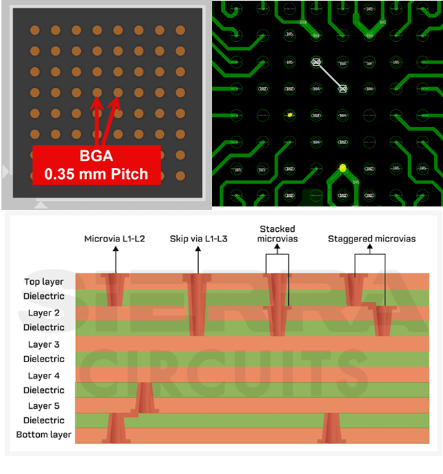
Figure 1: BGA escape routing cross-section view (credit: Sierra Circuits)
Routing a 0.355mm to 0.25mm pitch BGA demands aggressive via-in-pad placement, sub-3-mil geometries, and stacked microvias. At 0.4mm BGA pitch, designers have options. One or two traces can route between via pads; microvia and trace geometries at 4/4 mil (via/trace) provide workable margins. As pitch tightens to 0.35mm and approaches 0.25mm, these options collapse. The math becomes unforgiving: a 0.35mm pitch (13.8 mils) leaves approximately 4-5 mils between pad edges after accounting for minimum pad sizes, barely room for a single 3-mil trace with 1-mil clearance on each side.
Successful escape routing at these pitches requires a multi-pronged approach:
-
Aggressive via-in-pad: Every signal exits through its BGA pad via a filled microvia. No fan-out traces on the top layer beneath the component footprint are permitted, as every millimeter of top-layer real estate under the BGA is consumed by pads.
-
Sub-3-mil geometries: Trace widths at 2.5 mils or below, spaces at 2.5 mils, requiring fabrication capability at the edge of conventional HDI and pushing toward substrate-like manufacturing.
-
Maximum layer utilization: Every available routing layer under the device carries signals outward. Advanced 2-N-2 or 3-N-3 stackups become mandatory not for via depth but for routing channel count.
-
Stacked microvias for vertical density: Signals must transition through multiple layers within the tight confines of the BGA footprint. Staggered vias consume lateral space that doesn't exist.
HDI Considerations for Chiplet Interconnects and HBM
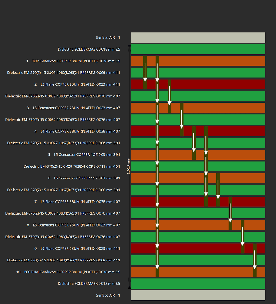
Figure 2: 10-layer PCB Stack-up cross-section for a complex AI PCB design, arrows indicate via layers (e.g. 1-2, 2-3, etc.) (NVIDIA Jetson AGX Orin 64 GB PCB)
Modern AI accelerators increasingly incorporate chiplet architectures where multiple silicon dies communicate through package-level interconnects, with HBM stacks providing memory bandwidth measured in terabytes per second. When these modules mount to a PCB, the board must support not just the module's external interfaces but also the power delivery and thermal management that enable chiplet-to-chiplet communication within the package.
The PCB beneath an HBM-equipped module faces unique challenges. Power density peaks beneath the HBM stacks, which may consume 10-20W each while occupying minimal footprint. Signal integrity requirements for the module's external interfaces (PCIe Gen5/6, high-speed Ethernet, display interfaces) demand clean power delivery with impedance below milliohms at frequencies into the hundreds of megahertz.
HDI stackup design for these applications must allocate sufficient plane pairs for power delivery, often dedicating 4-6 layers purely to PDN in the region beneath the module while still providing the routing layers needed for high-speed signal escape. This drives layer counts upward even as HDI efficiency reduces them elsewhere on the board.
Fan-Out Package Escape Patterns Extended onto the PCB
Fan-out wafer-level packaging (FOWLP) and fan-out panel-level packaging (FOPLP) redistribute a die's fine-pitch connections to a more manageable BGA pitch on the package bottom. But "more manageable" is relative as fan-out packages often present 0.4mm or 0.35mm pitch BGAs with very high pin counts.
The escape patterns developed for fan-out package design such as radial redistribution, orthogonal routing channels, ground-signal-ground (GSG) structures for RF signals extend naturally onto the PCB. Designers should study the package's internal redistribution layer (RDL) routing to understand signal groupings and maintain those groupings through the PCB escape.
Particularly for high-speed serial interfaces, the package and PCB form a continuous transmission line. Impedance discontinuities at the package-to-board transition degrade signal integrity; escape routing that mirrors the package's internal topology minimizes these discontinuities.
Thermal and Warpage Challenges in Dense Chiplet Zones
AI accelerator modules can dissipate 200-500W in a footprint smaller than a credit card. The PCB beneath such a module experiences extreme thermal gradients, potentially 50°C or more difference between the region directly under the module and board areas just centimeters away.
These thermal gradients create several challenges for HDI designs:
-
Localized expansion: The hot zone expands more than surrounding regions, creating mechanical stress at the boundary. Microvia interfaces in this stress zone experience accelerated fatigue.
-
Warpage during operation: Differential expansion bows the board dynamically during operation, stressing solder joints and potentially causing intermittent connections.
-
Material degradation: Sustained high temperatures in the hot zone can approach or exceed material Tg, softening the dielectric and potentially allowing copper movement.
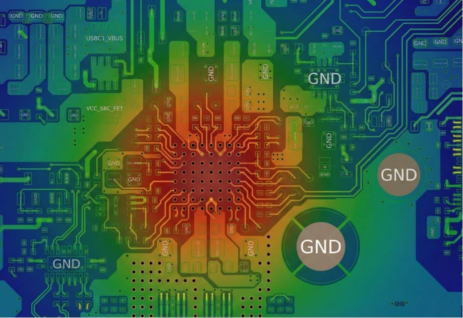
Figure 3: Thermal gradient under BGA component
Mitigation strategies include high-Tg, low-CTE materials in the module region, thermal via arrays connecting to internal ground planes that spread heat, copper balancing to minimize differential expansion, and mechanical design that accommodates dynamic warpage without overstressing solder joints.
When HDI Layers Mimic Interposer Functionality
Silicon interposers, which are thin silicon substrates with through-silicon vias (TSVs) that redistribute connections between chiplets and package substrates, enable the finest-pitch chiplet integration. But silicon interposers are expensive, and for some applications, aggressive HDI can provide interposer-like functionality directly in the PCB.
"PCB as interposer" designs push HDI to its limits: 2-mil or finer traces and spaces, 3-mil microvias on 2-mil dielectrics, any-layer via configurations, and substrate-grade materials. These designs blur the line between traditional PCB and IC substrate manufacturing, often requiring fabrication at facilities with both capabilities.
The trade-off is cost versus capability. A true silicon interposer with chiplet-scale (sub-50-micron) interconnects enables integration that PCB technology cannot match. But for applications where 100-150 micron feature sizes suffice, aggressive HDI PCB construction can provide adequate interconnect density at a fraction of interposer cost.
Designers approaching these limits should engage both PCB fabricators and substrate manufacturers early to understand where capability boundaries lie and which technology provides the best cost-performance trade-off for their specific requirements.
Links:
-
PCB Via types - https://resources.pcb.cadence.com/blog/an-introduction-to-microvias-in-pcb-design
-
How to Design Reliable Microvias in Your PCBs - https://www.protoexpress.com/blog/how-to-design-reliable-microvias-in-your-pcbs/