Why Decoupling Capacitor Placement Becomes Harder in HDI PCB Designs
If you have been designing PCBs long enough, you know that decoupling capacitor placement is one of those challenges that looks straightforward in a textbook and becomes progressively more painful as your board density increases. On a four-layer board with generous keepouts and 0.8mm BGA pitches, getting your decaps close to power pins is mostly a matter of discipline and good floor planning. But push into HDI territory with fine-pitch BGAs, stacked microvias, sub-0.5mm ball pitches, and 12-plus layers - the rules change in ways that are not always obvious until you are already in trouble.
Here is a breakdown of why HDI makes decoupling placement fundamentally harder, not just incrementally more constrained, and the technologies that can help overcome these challenges.
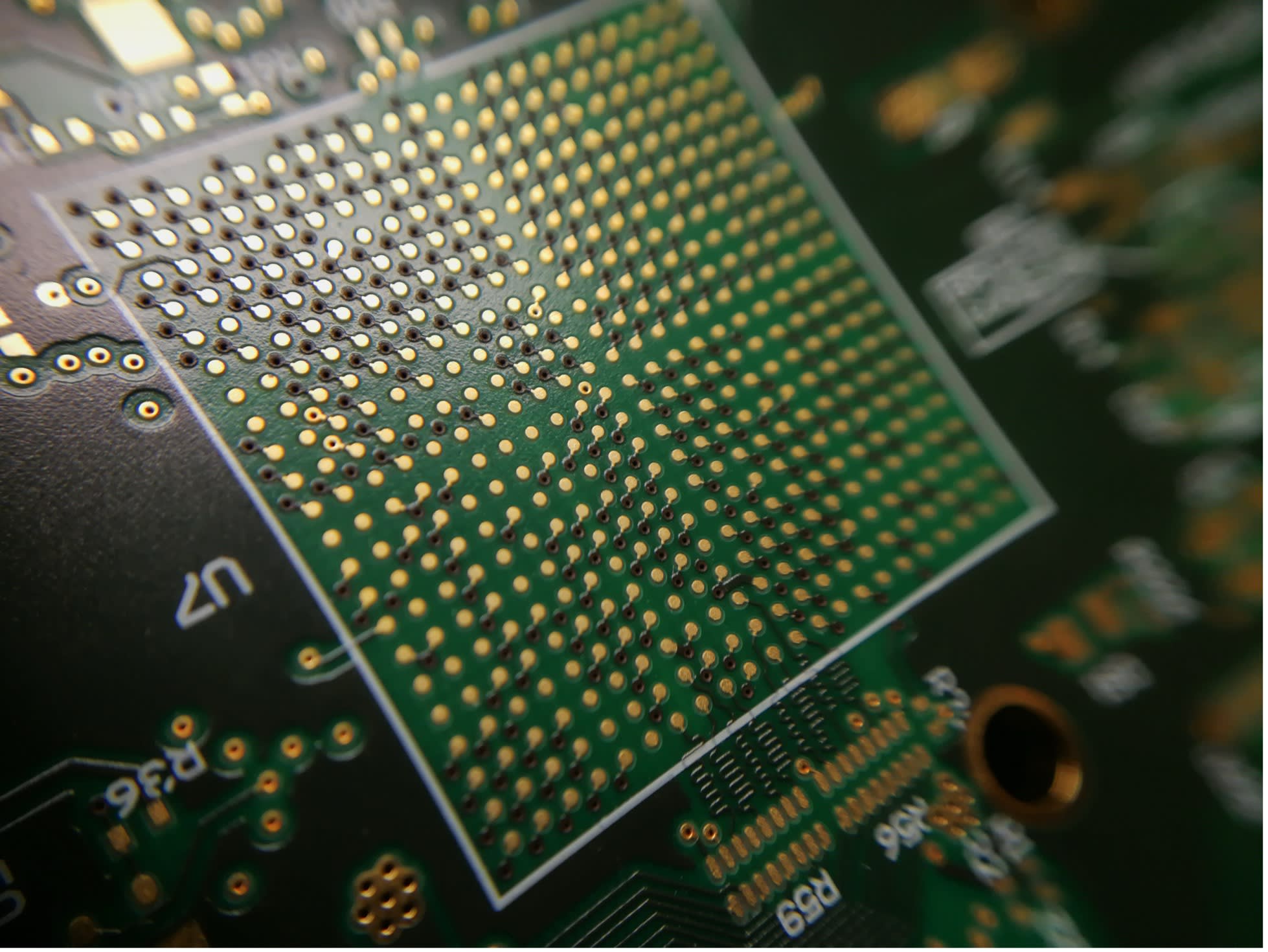
Figure 1: A high-density HDI PCB with fine-pitch BGA components. As board density increases, the constraints on decoupling capacitor placement compound significantly across every layer of the design.
The Core Problem: Physical Proximity Gets Harder to Achieve
The foundational rule of decoupling has not changed. The closer a decoupling capacitor is to the IC's power pin, the better it can respond to transient current demands, ideally within 1 to 2mm of the power pin to minimize loop inductance. In HDI designs, that proximity is exactly what the physical reality fights against.
The traditional approach creates a direct conflict: you need vias to escape BGA signals, but those same vias block capacitor placement on layer 2 or the bottom side. On a conventional board with dog-bone fanout, the routing escape routes consume the real estate where your decaps need to live. The vias are in the way before you even place your first capacitor.
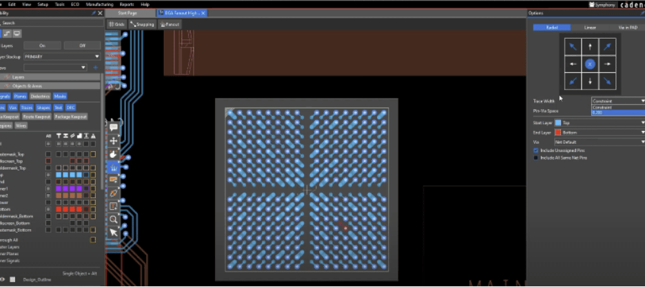
Figure 2: Traditional dog-bone BGA fanout routing occupies the interstitial space between balls where decoupling capacitors need to be placed, creating a direct conflict between signal escape and power delivery.
This is not a minor inconvenience. It is a structural constraint that forces tradeoffs between signal escape routing and power delivery, and those two objectives are both non-negotiable. As Eric Bogatin notes in his book, Signal and Power Integrity Simplified, every nanohenry of avoidable inductance in the decoupling path is a design decision, not an unavoidable consequence.
It is worth introducing a term here that will be central throughout this discussion: the Power Delivery Network, or PDN. The PDN encompasses everything from the voltage regulator to the IC power pins-planes, traces, vias, and decoupling capacitors alike. In HDI designs, the PDN is particularly sensitive to placement and routing decisions because the geometry of every element in that path directly determines how effectively power is delivered under transient load conditions. Keeping the PDN in mind from the very beginning of floor planning, not just during component placement, is what separates boards that pass signal integrity validation from those that require late-stage rework.
Fine-Pitch BGAs Shrink the Window for Via-in-Pad Relief
Via-in-pad technology exists precisely to address this conflict. Using via-in-pad maximizes the number of capacitors you can place under BGAs, reduces the space occupied by footprints, and minimizes inductance. When you route vias directly through the BGA pads, you free up the immediate space between balls for capacitor mounting vias, rather than competing with escape routing for the same surface area.
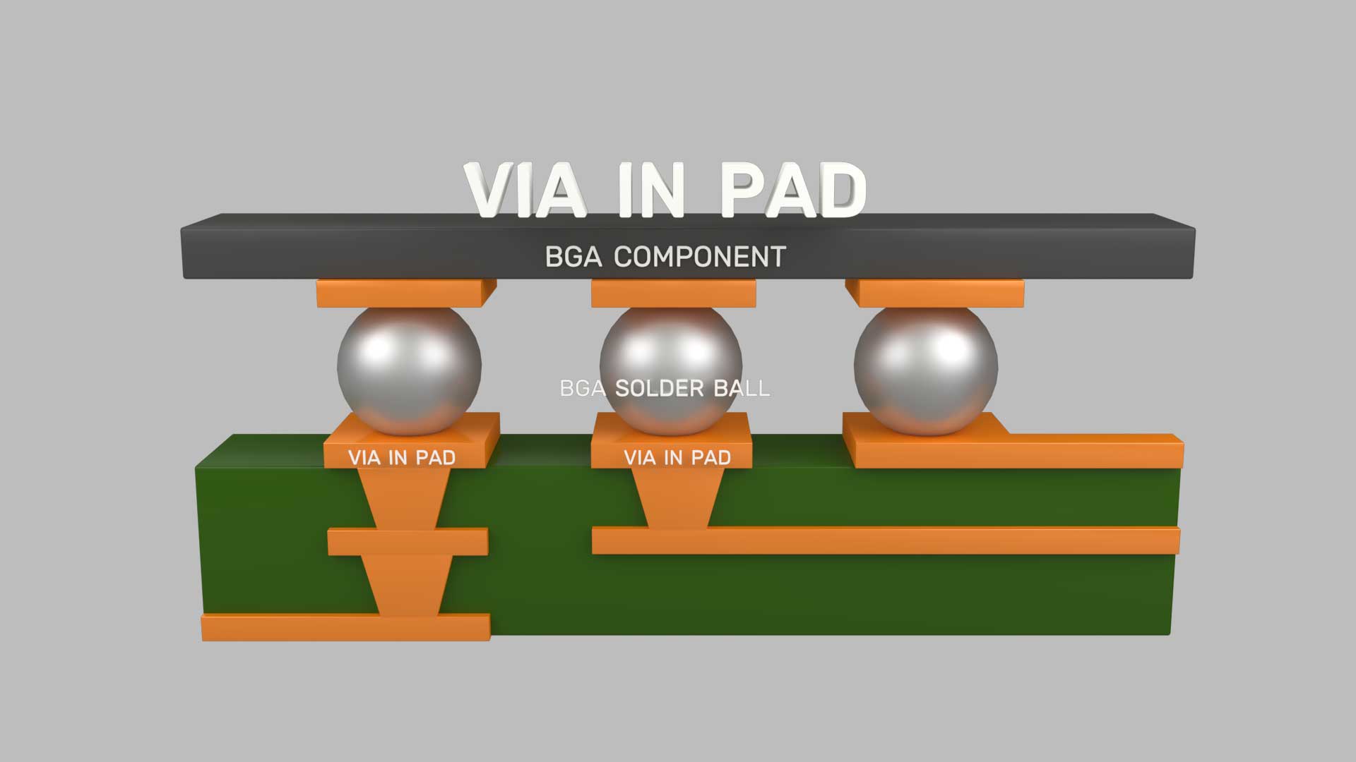
Figure 3: Via-in-pad cross-section showing a filled microvia routed directly through the BGA landing pad. This approach frees interstitial space for decoupling capacitor placement but requires filled and plated microvias and sequential lamination.
The catch is that via-in-pad becomes mandatory, not optional, as ball pitch shrinks. At 0.65mm pitch, dog-bone routing gets tight but may still work. Below 0.5mm, via-in-pad is your only realistic option. And once you are committed to via-in-pad on an HDI board, you are also committed to filled and plated microvias, sequential lamination, and the fabrication complexity that comes with it, all of which introduce their own constraints on where and how you can route power and ground connections to those capacitors.
It is important to recognize, though, that via-in-pad does not solve the decoupling problem - it shifts it. Freeing up intermediate space removes one constraint, but you may still find yourself without adequate placement area for the number and value of decaps the PDN requires. When that happens, the answer is not simply to use more via-in-pad. Instead, you may need to move to smaller capacitor packages such as 0201 or 01005 to fit more decaps in the available footprint, rethink the decoupling strategy entirely by distributing capacitors differently across layers, or in more extreme cases, evaluate whether a different IC package with a more favorable ball pitch or power pin distribution would better support the PDN requirements. Via-in-pad is a powerful tool, but it is the beginning of the placement solution, not the end of it.
Stacked microvias add another layer of consideration. Laminate and copper stress cracks become more likely in microvia stacks exceeding three high due to CTE mismatch between the copper structure and surrounding laminate. This is a reliability risk that needs to be weighed against the routing density gains during stackup planning, not discovered during qualification testing.
Loop Inductance: The Problem Compounds with Layer Count
Even when you get a decoupling capacitor physically close to the power pin, the inductance of the current loop, from capacitor to via to power plane to via to ground plane and back, determines how effective it actually is at high frequencies. The loop area is influenced by both the separation between the two vias and the distance between the capacitor and the plane layers. Distance to the plane and via separation are critical factors that need to be addressed to improve decoupling performance.
In a standard four-layer board, your decoupling cap will always be close to one plane layer and far from the other. There is not much you can do about that. But in an HDI stackup with many layers, you have more flexibility and more decisions to get wrong. If the board has more than four layers, you have some flexibility in optimizing the location of your decoupling caps relative to the power and ground planes, and you will lose a lot of distributed capacitance if you do not place power and ground planes on adjacent layers.
Smith and Bogatin in Principles of Power Integrity for PDN Design make this point precisely: the PDN is a distributed system, and the inductance of the current path from charge source to load determines the frequency at which that source becomes ineffective. In HDI, that path is determined by decisions made weeks before placement begins.
The higher the layer count, the more the stackup decisions made early in the design cycle constrain your power delivery options later. If power and ground planes end up separated by several signal layers because signal routing took priority, you are fighting against that decision every time you try to place an effective decoupling network.
There are concrete steps that help here. First, always consult the IC datasheet before finalizing your stackup. High-speed processors, FPGAs, and memory interfaces increasingly include PDN guidelines or reference stackups that specify recommended plane pair placement, decap values, and target impedance profiles. These documents are often the most direct guidance available on how to structure your power planes around a specific device. Second, establish the discipline of placing your power-ground plane pair adjacent to each other, as close to the device layer as your routing requirements allow. Third, if the stackup must accommodate a large number of signal layers, consider whether splitting the design into separate power and signal regions can protect the PDN plane geometry while still meeting routing density requirements.
Simultaneous Switching Noise and Ground Bounce
One failure mode that gets significantly worse in HDI designs and is directly tied to decoupling effectiveness is simultaneous switching noise. When multiple output drivers switch state at the same time, the resulting transient current demand creates voltage fluctuations on the power and ground rails that can corrupt signal integrity across the board. In a conventional design with large, continuous plane layers and generous decap placement, the local charge reservoir is usually sufficient to absorb these transients. HDI changes that calculus considerably.
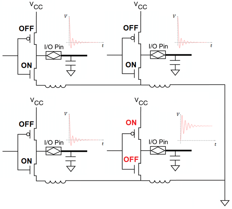
Figure 4: Simultaneous switching noise manifests as voltage fluctuations on the power and ground rails when multiple output drivers switch at the same time. In HDI designs with fragmented power planes and reduced distributed capacitance, the decoupling network must absorb these transients entirely.
In HDI designs, power planes are often divided into smaller sections due to increased signal routing layers, which raises PDN impedance and makes simultaneous switching noise and ground bounce more pronounced problems that decoupling placement must address. A fragmented power plane means the distributed capacitance you would normally count on is reduced, and the decoupling capacitors have to work harder to compensate. If those capacitors are not placed correctly relative to the switching outputs, or if their via connections add enough inductance to slow their response, the noise budget erodes quickly.
This is particularly relevant for FPGAs and high-speed processors in HDI designs where hundreds of I/O pins can switch simultaneously. Getting the decap placement right around the I/O power rails on these devices is as important as the core power decoupling, and the same physical constraints apply.
Space Compression Drives Competing Priorities
HDI designs are dense almost by definition. In dense PCB designs with BGAs or high-speed processors, balancing the number of decoupling capacitors with available board space is a common challenge. In practice, this manifests as a constant negotiation between the number of decaps the PDN analysis says you need and the physical space that actually exists after signal routing, thermal vias, connector keepouts, and mechanical constraints have all taken their share.
Core voltages can be as low as 0.8V with transient currents reaching hundreds of amps, and in these scenarios the target impedance of the power planes must be extremely low, below 1mΩ, to suppress voltage ripple. Meeting that target impedance requires a carefully planned combination of bulk capacitance, local high-frequency decoupling, and inter-plane capacitance. Each layer of that strategy has a physical footprint requirement, and in an HDI design, that footprint is competing with everything else on the board.
This is not something designers can assess by eye or resolve through intuition during layout. The interactions between plane geometry, capacitor placement, via inductance, and target impedance are too complex and too interdependent to evaluate informally. A correct-by-design approach quantifies tradeoffs before component placement is locked in-through pre-layout PDN simulation that establishes target impedance profiles and capacitor count requirements. These targets are then verified after routing through post-layout analysis to confirm the physical implementation meets them. Boards that skip the pre-layout step tend to discover their PDN deficiencies during compliance testing, at which point the fixes are expensive and the schedule impact is significant.
Capacitor Value Strategy Across Frequency Tiers
Most engineers know you need multiple decoupling capacitor values on a board. What HDI forces you to confront is that space constraints mean you cannot simply place all tiers everywhere and call it done. You have to be deliberate about which capacitor values get the premium placement closest to the IC, and which tiers can afford to sit further away without compromising their effectiveness.
Multiple decoupling capacitors of varying values are needed to filter different frequency components. Smaller capacitors in the 0.01µF to 0.1µF range address higher-frequency noise, while larger capacitors in the 1µF to 100µF range handle lower-frequency noise. In practice this means your high-frequency small-value caps need to be the ones winning the placement competition closest to the IC power pins, since their effectiveness degrades most sharply with distance and via inductance. The bulk capacitors can tolerate more distance and still provide adequate charge reservoir function for lower-frequency transients.
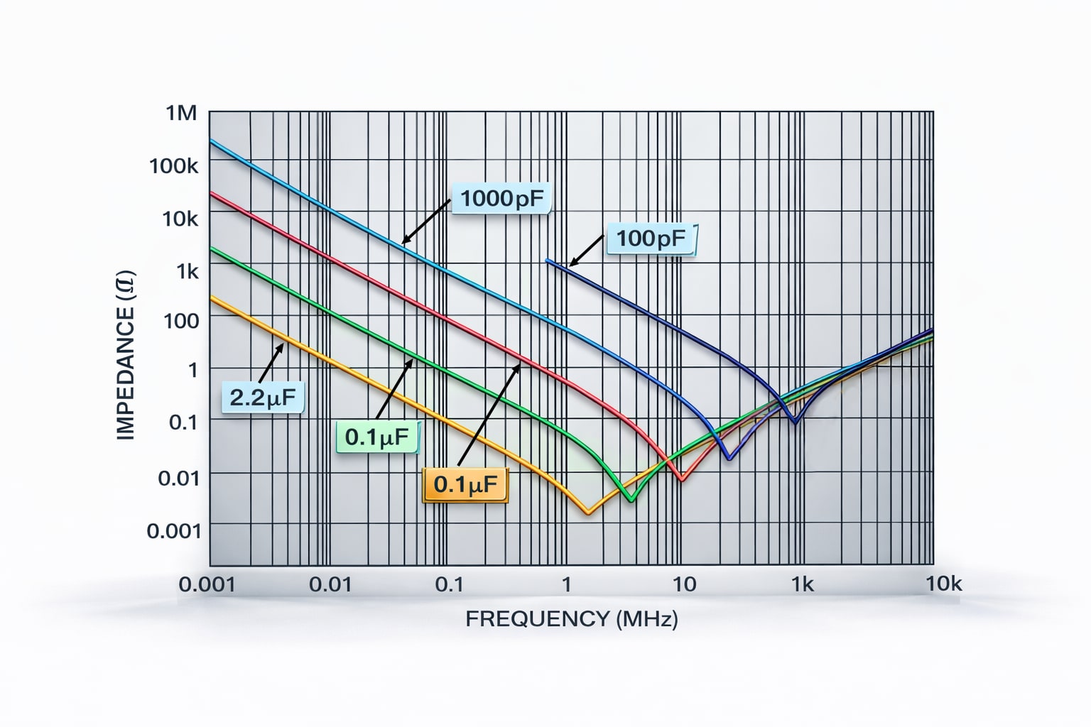
Figure 5: Decoupling capacitors of different values each address a specific frequency band. In HDI layouts where premium placement closest to the IC is limited, small-value high-frequency capacitors must win the placement priority since their effectiveness degrades most sharply with distance and via inductance.
The mistake that shows up in HDI layouts is treating all decoupling caps as interchangeable in placement priority. They are not. Tiering your placement strategy by frequency of operation rather than just by proximity to the IC gives you a more defensible PDN with less real estate consumed at the most congested locations on the board.
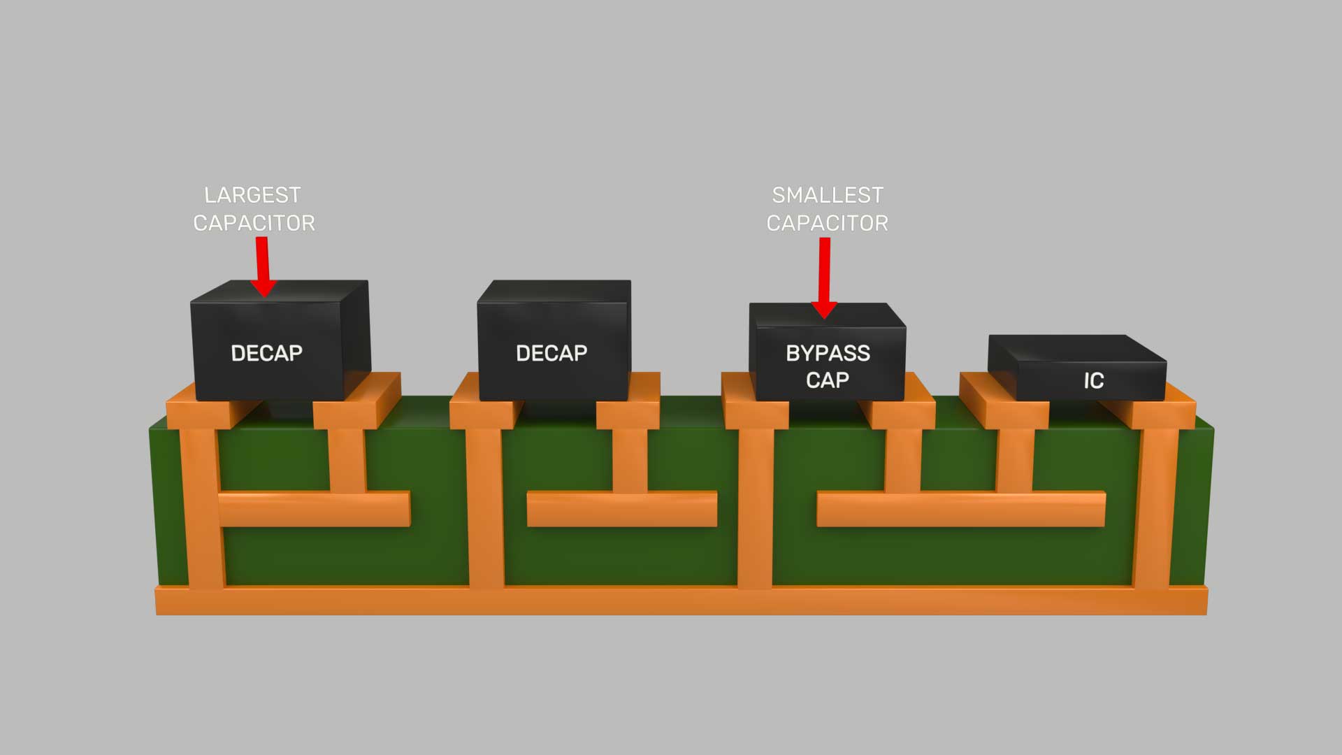
Figure 6: Decoupling capacitors should be placed according to the frequency range they support. Small value (typically 0.01μF-0.1μF), high frequency capacitors must be placed closest to the IC to minimize loop inductance, while larger “bulk” capacitors that support lower frequency energy can be placed farther away.
The Via Configuration Problem for High-Frequency Decoupling
At the frequencies that matter in modern high-speed digital designs, the inductance of the via connection to the power and ground planes matters as much as the capacitor's own parasitics. For high-speed circuits operating above 1 GHz, the decoupling capacitor's placement distance should ideally be less than one-tenth of a quarter wavelength at the capacitor's self-resonant frequency. Getting there in an HDI layout means via placement becomes dense enough that via-to-via clearance is a real constraint. Specifying a via-to-via clearance constraint that reflects your fabricator's minimum, alongside the rest of the design's physical spacing rules, lets the layout tool enforce that requirement continuously across the board so violations surface immediately rather than accumulating until a late-stage review.
Via-in-pad microvias connect IC landing pads directly to internal layers, improving power integrity by reducing parasitic inductance through shorter current loops and improving transient response so capacitors can respond more effectively to current demands. But stacked microvias add fabrication complexity and reliability risk, particularly around thermal cycling, that needs to be weighed carefully in the stackup planning process.
What Actually Helps
None of this means HDI decoupling is unsolvable. Using closely spaced, tightly coupled power and ground planes at 4 mils or less significantly reduces the dependency on precise capacitor placement because the planes themselves provide effective distributed capacitance. Pair that with symmetrical capacitor placement around or below ICs with multiple power pins to balance current distribution and reduce EMI, and you recover a significant amount of margin.
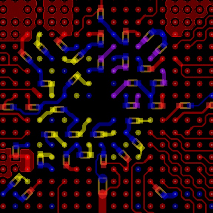
Figure 7: In fine-pitch BGA designs (example above is a 0.8mm pitch), 0201 decoupling capacitors can be placed on the opposite side of the PCB directly beneath the device to minimize current loop length and via inductance. This placement enables efficient high frequency decoupling by providing short, direct connection between the IC power pins and the power/ground plane pair, when topside placement is limited.
For boards where surface real estate is truly exhausted, embedded capacitance technology is worth serious consideration. Embedded capacitance technology integrates the capacitor function directly into PCB layers, saving surface space while significantly improving electrical performance by reducing inductance and resistance paths. Rather than mounting discrete capacitors on the surface and routing vias to reach the planes, embedded capacitance puts the decoupling function inside the stackup itself, as close to the planes as physically possible.
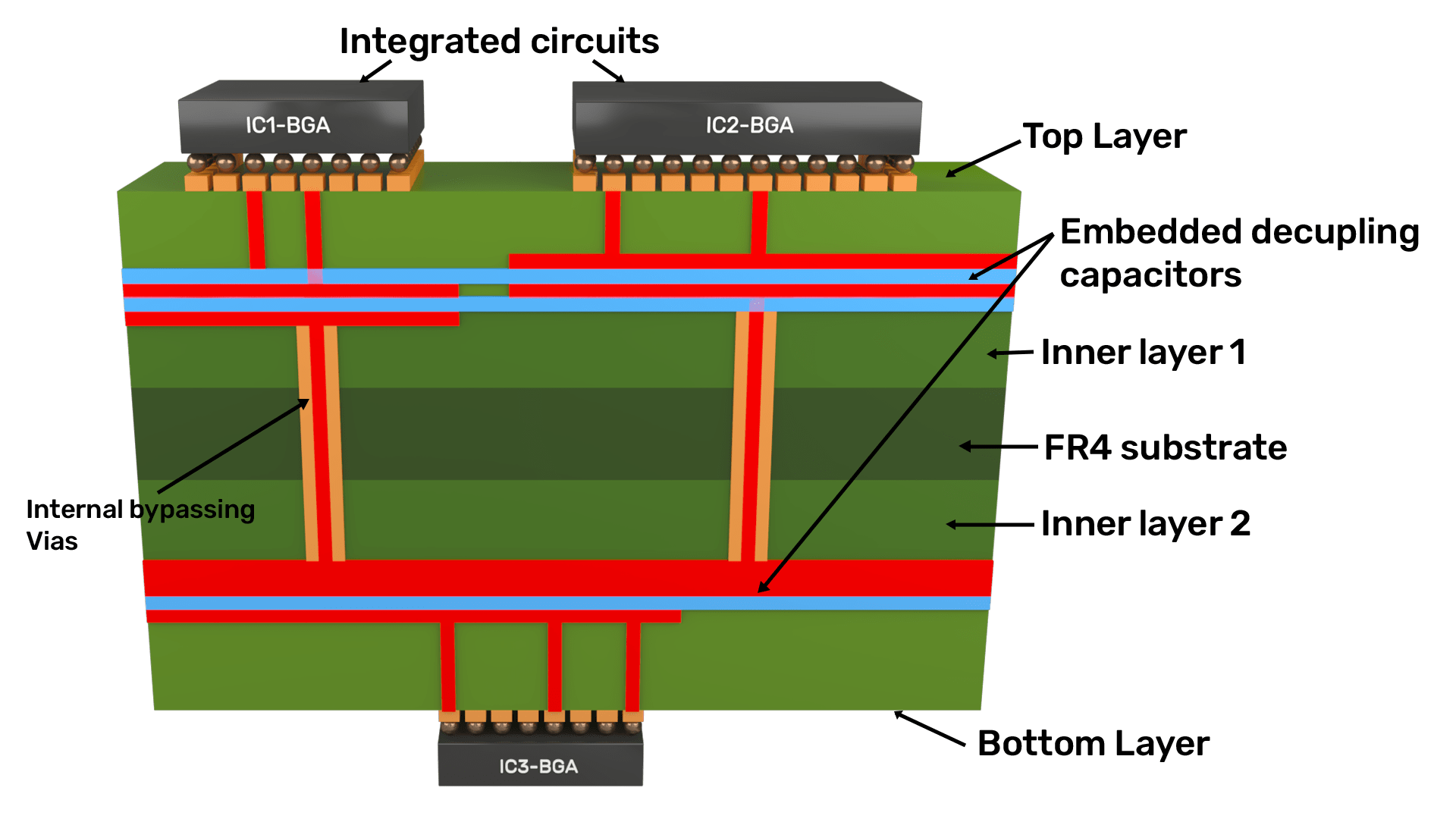
Figure 8: Embedded capacitance technology integrates decoupling directly into PCB layers, eliminating surface mounting and via connections entirely. This approach reduces loop inductance to near zero for the embedded tier while freeing surface real estate for components that must reside there.
The most comprehensive approach treats decoupling as a three-tier system rather than a single problem. This multi-layered strategy combines low-frequency decoupling handled by bulk discrete capacitors, mid-to-high-frequency suppression enabled by embedded capacitors in the PCB or package, and on-die capacitance for ultra-high-frequency stabilization. Each tier addresses a frequency range that the others cannot cover effectively, and in an HDI design where surface placement is constrained, offloading mid-frequency decoupling to embedded layers frees up surface real estate for the components that genuinely need to be there.
PDN simulation early in the design cycle is not optional on an HDI board. Doing it after component placement is already locked in means you are patching a problem rather than solving it. Running impedance analysis before finalizing your stackup and iterating on plane pair placement and capacitor count together rather than sequentially, is the approach that consistently produces better outcomes.
Bottom Line
Decoupling in HDI is harder because of every variable you normally control. The physical proximity, loop geometry, available surface area, and via configuration become more constrained at the same time your performance requirements go up. The PDN, which must deliver clean, stable power from the voltage regulator to the IC across a wide range of frequencies and transient conditions, is the system that ties all these variables together. As introduced earlier, the PDN encompasses more than just the planes and decaps in isolation; it includes the entire current path, with every geometric and material decision in the stackup influencing its behavior.
Add in fragmented power planes driving simultaneous switching noise, the need to tier your capacitor value strategy by frequency, and the fabrication complexity of via-in-pad and stacked microvias, and you have a problem that rewards early, systematic thinking and punishes late corrections. Via-in-pad and other HDI techniques shift constraints rather than eliminate them, and the correct response when physical placement runs out of options is to revisit package selection, capacitor sizing, or embedded capacitance solutions-not to keep adding vias and hoping for the best.
The physics has not changed. The margin available to work with has. Getting it right requires treating PDN design as a first-class constraint from the start of floor planning, validated through pre-layout simulation and confirmed through post-layout analysis, not a cleanup pass after signal routing is done. On an HDI board, by the time you are trying to fix your decoupling network, the decisions that determine whether you can fix it have already been made.