PCB Design For Signal Integrity: Digital Transmission Lines
The definition of high speed interconnect changes as time goes by. The same principles apply but to an even greater degree. Hallmarks of high-speed digital routing include:
- Timing budgets based on data lanes matching a clock in terms of time of flight
- Phase matching within a differential pair along the entire length
- Impedance control based on reference planes, line width and spacing
- Transitions from outer to inner layers as necessary
- Isolating aggressor signals from victims
The first step in creating a compliant data bus is to just route the connections. You want to know what you’re working with. Probing the unrouted ratsnest provides a high level of abstraction that may not be a reliable indication of the final routing. Ideally, all of the members of the bus will follow the same routing pattern in terms of the layers used.
Figure 1. Differential pairs should have a pair of ground vias in close proximity wherever they transition from the outer layer to an inner layer. Symmetry is better but not always possible. Adding them as you go will help. Image Credit: Author
The number of vias for each member of the bus, including the clock, should be the same. Vias matter because each one creates a discontinuity. Also, routing internally helps contain EMI and leaves the outer layer board space for components.
Signals travel faster on those inner layers so it helps to dive down into the board as soon as possible. Setting a value for the Maximum Exposed Length will help ensure that the length readings translate to accurate timing while cutting down on noise. There may be serial resistors or termination resistors that complicate the length calculations.
The Clock is the Boss of the Digital Realm
Once the connections are there, a survey of the line lengths will indicate the longest routes. At this moment, the clock net is probably both too long and too short to meet the requirements. What that means is that the group has too much variance. Using the Highlight command to paint the ones that are naturally longer than the clock will inform the work to follow.
Anything you can do to shorten the longest ones will help resolve the routing of the shortest ones with a minimum of meandering. Shorter is better to cut down on signal degradation. Once the longest trace has been routed as short as possible, you have a good idea of how long the clock has to be.
This is where the constraint manager comes in. The primary constraint to create is the Relative Propagation Delay. Creating the match group and assigning the “target” is the first step to resolving the timing budget. Generally speaking, the target will be the clock net. There are times when the clock is a single ended line and others where two signals are paired up. When it’s a pair, phase matching is critical. If the two lines are exactly the same length, you get the most leeway for the rest of the group.
Two Strategies For Length Matching Buses
You can choose to match the clock to the length of the longest trace or use up the allowable skew to make the clock shorter. The second option creates a brittle design where one more via can break the timing budget. Board size may be such that using the available tolerance is the only way to complete the layout. We’re being pulled in two directions.
That said, I’ve never been in a design review where they’ve criticized the layout for perfect length matching. On the other hand, 126 matched lines with two going slightly longer, but within the specification, did get a comment. I messed around with the fanout then tightened up those two signals by routing outside of the 45 degree angles rather than lengthen the rest.
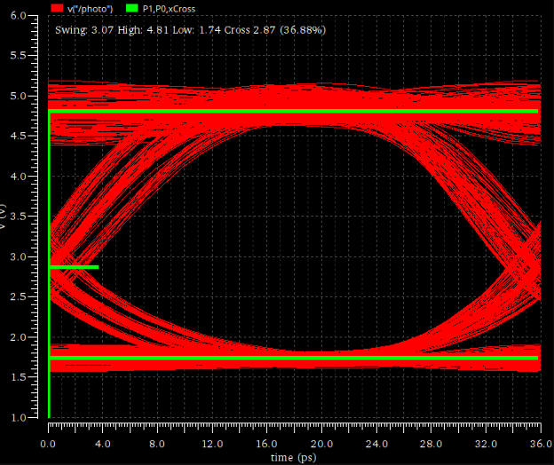
Figure 2. Analyzing a bus results in an eye-diagram. The coin of the realm is open eyes noted by the large space in the center.. Overshoot, undershoot, ripple and other issues become apparent to the technician. Image Credit: Cadence
Phase Matching Differential Pairs
When it’s time to drop the signals into the inner layers, signal integrity wants the differential pair to have the vias placed as close as allowable by the design rules. The gathers should be symmetrical to form a Y rather than the y shape.
This is not the place for phase matching by bending one trace while the other one goes straight. Over the years, I’ve found that using a rounded bump for phase matching is more efficient than using diagonal lines. The rounded lump seems to add more length for the amount of space taken.
We do like the phase matching to be near the location of the mis-match. The two members of the pair get out of sync when they make a bend. A bend in the opposite direction will cancel out the first bend so it’s a wash. Doing a U-turn will double up the intra-pair skew.
The U-turn may be unavoidable when the origin and the destination pins do not align in terms of positive and negative sides of the diff-pair. That’s where I would add the “speed bump” so as to cancel the phase mismatch where it happens.
Loosely Coupled vs. Tightly Coupled Differential Pairs
Loosely coupled pairs are common for Display Port, HDMI, MIPI and other high bandwidth applications. By definition, loosely coupled means that the gap between the two lines is greater than the line width. More skew occurs due to the difference in path lengths around bends.
We have two signals propagating along the same path. If one gets substantially ahead of the other, a transient voltage spike would affect the two lines differently. The shockwave hits one and not the other if the signals are too far apart. We lose the cancellation that is the main reason for diff-pairs in the first place. Managing the two wavefronts of the differential pair so that they run alongside each other from end to end is known as dynamic phase matching.
Figure 3. Clock nets (painted yellow) are segregated by ground planes (green) as much as possible while other traces may be mashed together. All of the loosely coupled differential pairs enjoy a gap that is three times the thickness of the dielectric between this layer and the adjacent ground planes. That value is also nearly equivalent to the trace width. Image Credit: Author
Lumping the phase matching at one end or the other is called static phase matching. Tightly coupled differential pairs with lower rise times will be more resilient to the issues described above. While all of this applies to Data, Address, Control, Strobe and others signals in a bus, the Clock stands out as the one continuously flipping the bit. We take extra care by setting it apart in a faraday cage of its own.
Single ended digital transmission lines are more likely to require a termination resistor to soften the landing at the end of the line. Reflections are one of the ways that signals get degraded. Longer lines obviously have more chances to run into interference issues. As edge rates and line length increase, we’re bound to seek out higher performance materials for dielectrics.
Spacing rules will also become more stringent. Vias can have a more onerous effect. We can mitigate this by back-drilling vias to remove stubs in the z-axis. This is especially true of the thick backpanels that support multiple processor boards.