How to Design Reliable Analog ASICs
Key Takeaways
-
What are the major types of ASICs?
-
What are the differences and similarities between designing components and designing PCBAs?
-
Design tips for reliable analog ASICs.
A common type of ASIC.
When I was younger, I recall hearing some of my elders allude to the fact that teenagers can be somewhat resistant to taking advice. These assertions would sometimes include, “...a little bit of knowledge is a dangerous thing.” The implication here was that as people begin to scratch the surface of intellect, they assume a greater level of understanding than they actually have, which can lead to incorrect assumptions and perhaps, unpleasant consequences.
The other side of the coin, which trainers, instructors, and teachers are keenly aware of, is the tendency of people to compartmentalize their knowledge. This can lead to the inability to realize how things that may fall under different subject headings are actually interconnected. A good example of this is not considering the chemical study of the movement of electrons between valence bands to be the current flow through electrical circuitry.
A similar disconnect can exist between the design of circuit boards and components. This is understandable, as components are typically selected for board design and then effectively placed for the best operation. ICs are usually among these selected components. However, there are times when special functionality is required and ICs must be designed. It may be surprising, but designing these devices has a lot in common with designing PCBAs. After taking a look at common application-specific ICs (ASICs), we will compare board and analog ASIC design to determine how best to design these special components for reliability.

Types of ASICs
If you bring up the subject of IC design, the first thing that comes to mind is probably a chip with like components that fit into one of the following classes.
Classes of ICs
→ Small scale integration (SSI): <100 components or ≅10 logic gates
→ Medium scale integration (MSI): <500 components or 10-100 logic gates
→ Large scale integration (LSI): 500-300000 components or > 100 logic gates
→ Very large scale integration (VLSI): > 300000 components
Terms such as very very large scale integration (VVLSI) and ultra large scale integration (ULSI) are sometimes used to indicate even greater component densities, yet it is more common to use VLSI as a catch-all phrase for all of these.
In addition to classification based upon scale, ICs are also categorized according to the amount of customization. ICs where some degree of customization is possible are termed ASICs, as they allow or require the designer to customize the IC for specific functionality or applications, as shown below.
Types of ASICs
➢ Full-custom
➢ Semi-custom
• Gate array
• Standard cell
➢ Programmable
• FPGAs
• PLDs
The examples listed, including FPGAs and PLDs, are very common ASICs and their usage removes some design responsibilities from the designer, such as component placement within the IC and IC package design.
Designing Boards vs Designing ASIC Components
Depending upon the type of ASIC the application requires, its design may be quite similar to designing a PCB layout, as the following table illustrates.
* A standard IC package may be selected or a completely new package designed.
As shown above, the design of an ASIC is comparable to designing a PCBA layout. For full custom ASIC design, there is little difference, while for programmable ASICs there are minimal layout requirements. Instead, for FPGAs and PLDs, the challenging task is to select the proper interconnections and external components to achieve desired operational functionality. In either case, reliable operation is always a prime objective.
Designing for Analog ASIC Reliability
Semi-custom and programmable ASICs are primarily comprised of transistors, which are comprised of logic gates. Therefore, at the most basic level, these components operate as digital devices. Nevertheless, ASICs often are mixed-signal components that work with both analog and digital circuitry. When this is the case, the components may be referred to as analog ASICs. When designing these components, many of the same concerns that accompany analog PCBA design must be taken into account, as listed below.
Analog ASIC Design Tips
∿ Determine the best package type
The choice of IC package type is important as it determines whether a custom design is required. If at all possible, it is preferable to opt for a pre-existing package design. IC package design is an advanced capability that necessitates you to have the right PCB design tool, such as Cadence’s Package Wizard shown below.
Component package design wizard.
∿ Ensure layout passes DRC
If routing and layout is required, it is critical that you design to optimize signal integrity and minimize EMI problems, just as required for PCBA design. The best way to accomplish this is by making use of DRC guidelines for the ASIC. Just as for board design, ASIC designs need to be verified for manufacturability, which requires advanced capabilities such as those available with Cadence’s Virtuoso.
∿ Perform simulation and analysis
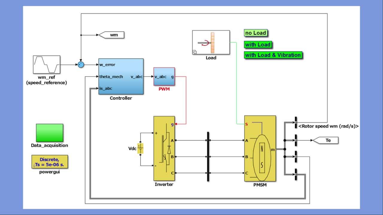
One of the best ways to optimize ASIC development is to ensure performance and functionality during the design and prior to fabrication. To accomplish this, the design is analyzed through simulation using a tool such as PSpice, as shown below.
PSpice-Matlab co-simulation of ASIC example.
As shown above, PSpice can be used in conjunction with other industry-standard tools, such as Matlab, to perform higher-level system analysis of your analog ASIC design.
The ability to design custom ASICs, including analog or mixed-signal chips, provides the designer with a great deal of freedom to optimize the design for the intended application. However, a PCB Design and Analysis platform that includes the necessary advanced capabilities is needed--including Analog/Mixed-Signal Simulation available with PSpice.
If you’re looking to learn more about how Cadence has the solution for you, talk to us and our team of experts.