Allegro X Advanced Package Designer SiP Layout Option Datasheet
Enhanced capabilities for multi-chip packaging technologies
System-in-package (SiP) implementation presents new hurdles for system architects and designers. Conventional EDA solutions have failed to automate the design processes required for efficient SiP and advanced packaging development. By enabling and integrating design concept exploration, capture, construction, optimization, and validation of complex multi-chip and discrete substrate assemblies, Cadence SiP design technology streamlines the integration of multiple high-pin-count chips onto a single substrate, necessary to design high-performance and complex packaging technologies.
Cadence SiP Technology
Designers of high-performance electronics are turning to advanced package design because it offers a number of significant advantages such as increased functional density, integration of disparate chip technologies, low power, improved signal performance/integrity, and ease of integration into an overall system. However, this level of design also requires expert engineering talent in widely divergent fields, which historically has limited adoption by the mainstream industry.
By streamlining the integration of multiple high-pin-count chips onto a single substrate through a connectivity-driven methodology, the SiP Layout Option allows designers to adopt what were once expert engineering design capabilities for mainstream product development. Cadence IC Packaging solutions seamlessly integrate with Cadence Innovus technology for chip/package interconnect refinement and Cadence Virtuoso technology for schematicdriven RF module design.
SiP Layout Option
The SiP Layout Option enhances the constraint- and rules-driven layout environment of Cadence Allegro X Advanced Package Designer to design high performance and complex packaging technologies. It adds a powerful set of auto-interactive flow, routing, and tuning features that speed planning, optimizing, instantiation, and timing closure of critical interconnects (e.g., DDR memory, high-speed serial, silicon substrate, and graphic interfaces). Intelligent route flow planning and automated breakout tools reduce time-consuming and tedious manual breakout and routing tasks and optimize large bus routes to use minimum space and layers. The SiP Layout Option also adds additional automatic routing capabilities based on Specctra technology for siliconbased substrates.
The full suite of comprehensive Allegro PCB DesignTrue DFM Technology and assembly rules improves substrate yield and prevents manufacturing and assembly issues. The option supports the assessment of manufacturing variation, and the creation of design variants with different substrate stack-up, die stacking, and wire bond configurations derived from the same master design. The option also enables a bi-directional flow with the Virtuoso platform for IC/package co-design.
Benefits
- Allows connectivity assignment and optimization between ICs, components, and substrate for minimal layer usage based on signal integrity and routability
- Includes comprehensive substrate design for manufacturing (DFM) capabilities for rapid manufacturing preparation
- Creates bonding and stacking variants from a base design; assesses process variation (e.g., line width) impact with respect to design rule checks and system performance
Features
Interface-Aware Design
In advanced packaging design, you are likely turning to protocols such as DDRx, HBM, graphic, and high-speed serial buses to support the performance, power, and bandwidth requirements of your products. Are your layout tools delivering the speed and ease of use you need to keep pace with your design cycle demands? What if you could apply a hierarchical interfaceaware approach to accelerate your implementation process—and increase design quality, performance, and reliability along the way?
Interface-aware design capabilities let you design packages at a much higher level of abstraction, so you can achieve faster routing of standards-based interfaces. Traditional design authoring tools work with buses or bundles and a single-level hierarchical definition of a group of signals. However, today’s interfaces can’t be modeled in a single-level hierarchy. Other challenges to address include the increasing number of constraints, increasing design density, shrinking bump and pillar pitches along with an increasing number of large pin-count devices, and increasing time to route designs (in the face of shrinking design cycle time and resources).
To connect interfaces quickly and easily, the hierarchical interface-aware design capability in the SiP Layout Option:
- Enables authoring at a higher level of abstraction to improve productivity
- Passes interface definition to layout designers
- Guides critical component placement and enables route planning
- Allows the use of auto-interactive technology to further accelerate breakout, routing, and tuning of interfaces
The capability makes use of “flows”, which allow you to instantiate interfaces and hierarchical netgroups, configure and connect interfaces to components and blocks, assign routing layers, and swap assignments for routability and escape.
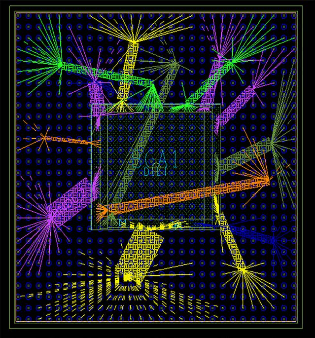
Figure 1: Buses and interfaces are represented by “flows”, simplifying planning and optimization of assignment and routing.
Auto-Interactives and Auto-Routing
The SiP Layout Option adds a full set of auto-interactives to quickly design complex, critical interconnects, including high-speed interfaces and buses in IC package design. Tools are provided to assist in the planning and breakout of die bump and ball patterns. Additional tools address timing, delay, and phase tuning of bus elements, giving visual indication where there are issues, and providing the tools to correct them. Specctra-based auto-routing is included for foundry and silicon-based substrates. These capabilities reduce the tedious, time-consuming, and manual breakout editing and connectivity
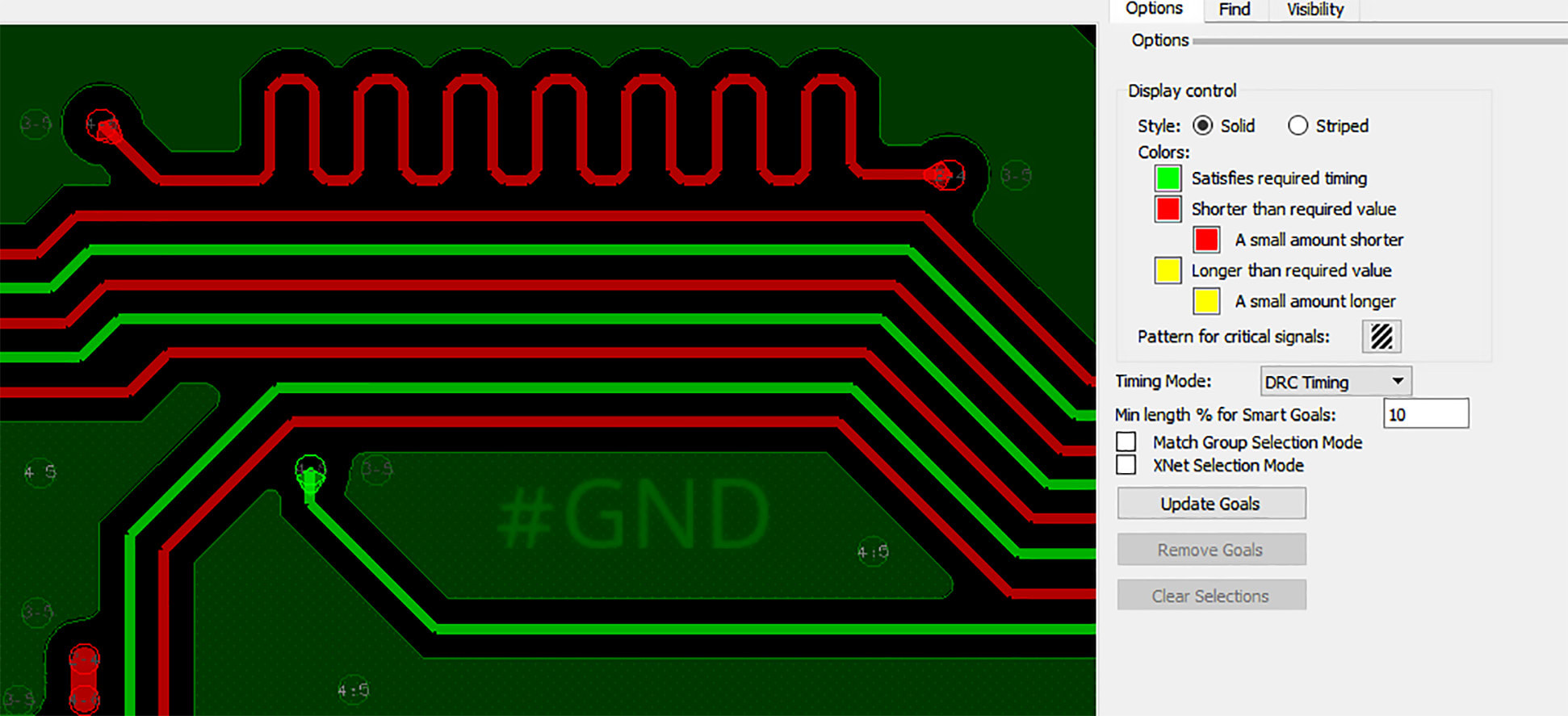 Figure 2: Quickly assess and correct differential pair and bus phase, delay, and timing.
Full Access to DesignTrue DFM Technology and ARC
Integrated into Allegro X Advanced Package Designer is an online advanced-language rule-checking engine that can eliminate tedious traditional post-design manufacturing mask checking. This engine can substantially reduce time to manufacturing readiness, streamlining the design process and empowering the package designer. Custom DRC rules can also be written and encrypted using the optional rules developer toolkit.
The SiP Layout Option adds a comprehensive assembly (and manufacturing) rule checker (ARC) providing more than 50 IC packaging-specific checks, including complex wire spacing and crossing rules. Checks can be executed as a check-group, individually, or as a custom selection; results appear in the Constraint Manager DRC tab, the DRC browser, and as graphical markers in the design. Likewise, this option gives access to the full suite of comprehensive DesignTrue DFM rules, improving substrate yield and preventing manufacturing and assembly issues. DesignTrue DFM technology lets you actually design for manufacturability—not redesign for manufacturability, not make frequent changes for manufacturability— and accelerate new product introduction. Define your manufacturer’s rules before you start and apply them in real time as you design. That way, when you’re finished with the design, you’re already ready for first-pass DFM signoff.
Manufacturability rules are easy to manage and collaborate on. Just like electrical constraints, the easy-to-use spreadsheet interface is intuitive for engineers and non-engineers alike, which makes re-use easy. The constraints are highly configurable with the ability to enable and disable groups and whole categories of rules, or individual rules. Rules can be applied in etch mode, non-etch mode, and in stack-up mode, giving designers the ability to isolate layers, geometries, and cutouts.
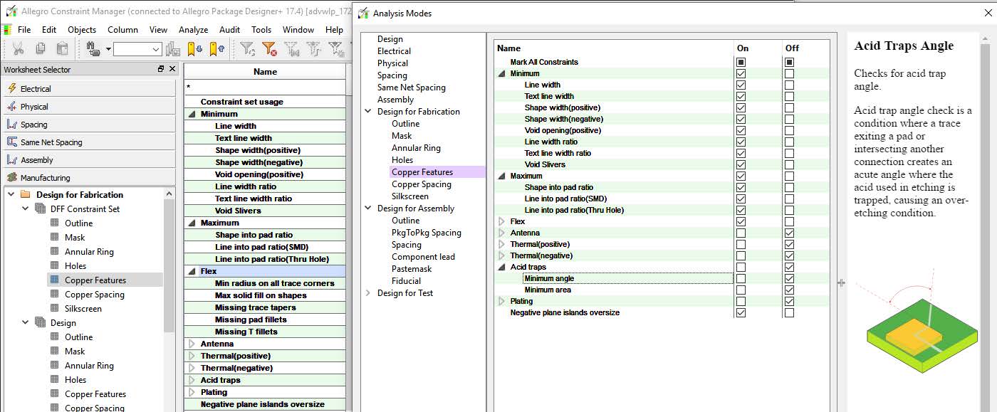 Figure 3: DesignTrue DFM technology checks your design for manufacturability.
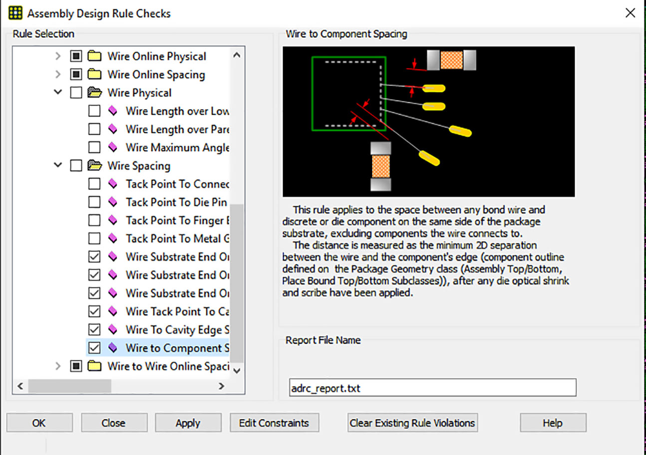 Figure 4: ARC checks complex wire interaction and package-specific rules.
Design and Process Variants
It is common for one package substrate design to have multiple configurations, both in die members and stacking variations, or in how the die are bonded out. The SiP Layout Option allows the designer to create one master design, spawn sub-ordinate designs representing each variant, and then assess the different bonding and stacking option designs for physical DRC, wire DRC, and signal integrity. Likewise, the option supports the assessment of physical manufacturing variation on DRC and signal integrity.
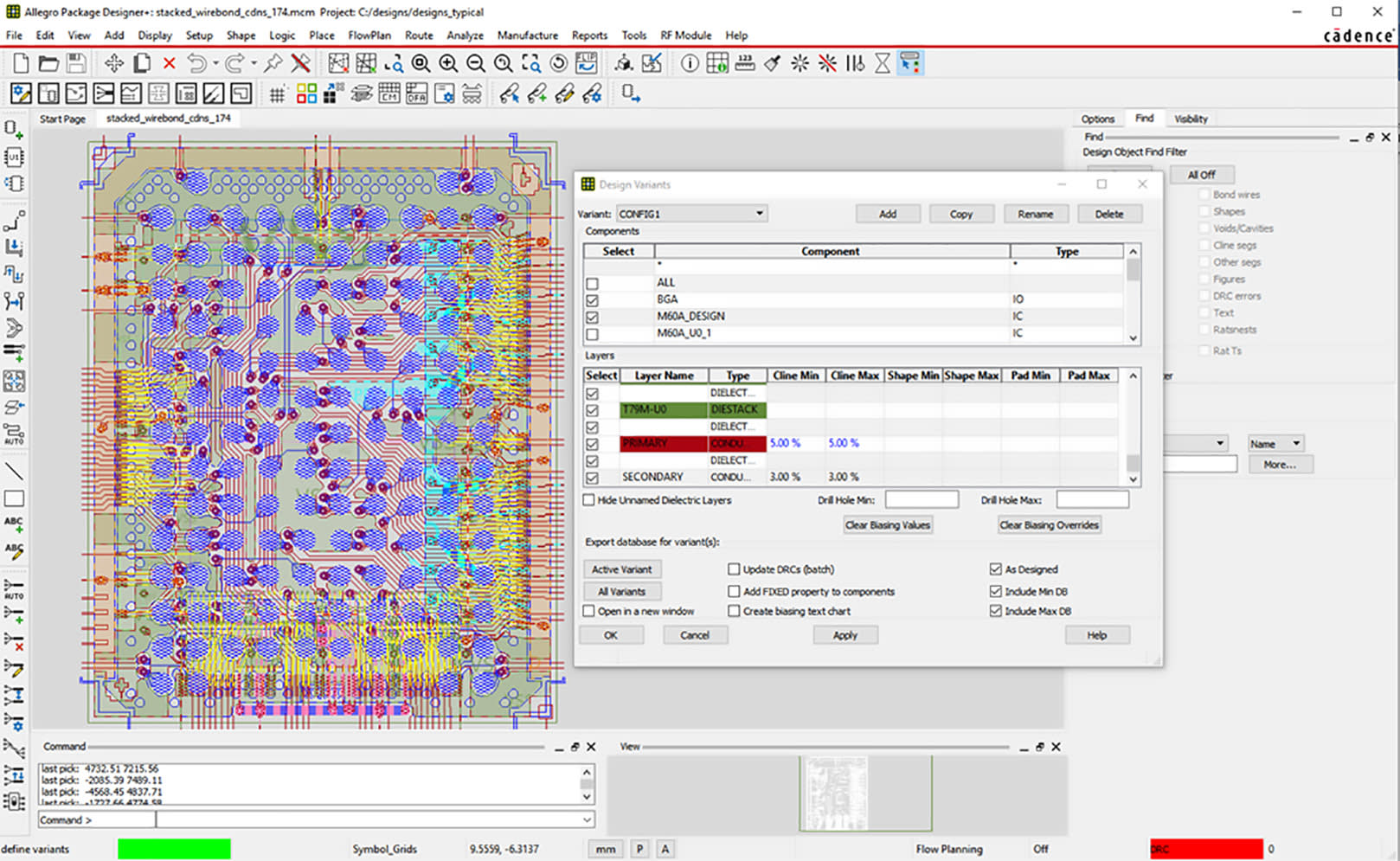 Figure 5: Design variants can be created with different die stack and bonding options. Designers can also assess the impact on manufacturing variation (e.g., line width) on performance and manufacturability.
Cadence Services and Support
- Cadence application engineers can answer your technical questions by telephone, email, or internet. They can also provide technical assistance and custom training.
- Cadence-certified instructors teach more than 70 courses and bring their real-world experience into the classroom.
- More than 25 Internet Learning Series (iLS) online courses allow you the flexibility of training at your own computer via the internet.
- Cadence Online Support gives you 24×7 online access to a knowledgebase of the latest solutions, technical documentation, software downloads, and more.
- For more information, please visit support and training .