How to Put Pins in Sections Using OrCAD X
Key Takeaways
-
Designers may wish to split a component across multiple parts when dealing with large pinout packages.
-
Changing the “Parts Per Pkg” value and setting “Package Type” to “Heterogeneous” in the “New Part Properties” dialog allows designers to distribute the pins of one component between multiple parts.
-
During placement, the part will increment through the sections of the package.
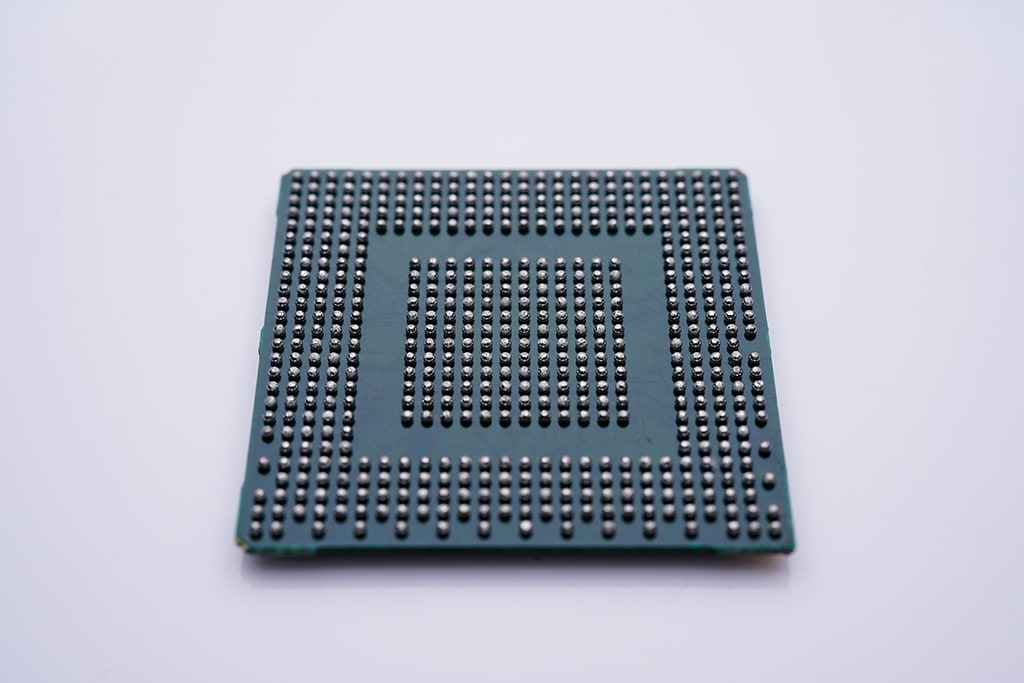
Wondering how to put pins in sections using OrCAD X for dense pinout packages like BGAs? Read on.
PCB layout arranges components, traces, and vias on the board to meet the desired engineering specifications and optimize performance. Mistakes or poor design choices made during the layout may lead to a new revision and manufacturing run; this can be aggravating during board development (i.e., prototyping) and disastrous during high-volume lots. In general, designers pay less attention to the arrangement of schematic symbols and wires, as these represent only logical, not physical, circuit information.
However, a well-designed schematic is conducive to an accurate and expeditious board layout. One of the many ways designers make schematics easier to digest is by splitting up parts across multiple pages when they have significantly high pinouts or dispersed functionality among multiple semi-independent circuit blocks. Designers looking to learn how to put pins in sections using OrCAD X Capture CIS can rapidly develop their schematics to benefit the layout and, ultimately, the board.
Overview of Multiple-Part Package for OrCAD X Workflow
|
1. New Part |
Add a new part to the project library, indicate how many sections it needs, and select heterogeneous to enable independent design of the multiple parts within the package. |
|
2. Design |
Separate the pinout to suit the schematic page(s) best. Follow all pin naming/numbering provided by the manufacturer. |
|
3. Placement |
Multiple-part packages progress alphanumerically through each section (depending on the part numbering system selected) when placing a part in the schematic. |
Why Split Pins into Sections?
The schematic acts as the blueprint for the board layout, pending additional instructions from the engineering team or manufacturers’ notes. However, the schematic is an abstraction of the layout: it does not tell designers where components and connections go, just how they will connect. This wrinkle allows for significant flexibility in a schematic design: consider the simple case of a multi-channel op-amp. All channels share the same rails (+VCC and -VCC/GND), but the paired inputs (inverting and noninverting) and output are distinct. It makes sense to illustrate the schematic symbol as if it were originating closer to the signal destination for multiple reasons if the signals from one component terminate at different sections of the board (i.e., memory, power, control, etc.):
-
The schematic doesn’t have to use as many off-page connectors. While off-page connectors are necessary to connect different sections of the circuit electrically (read: logically), they can make reading the schematic difficult due to the information distributed across multiple schematic pages. It’s easier to disseminate the nearby components for component grouping during layout to plan the early design stages.
-
For especially large pinouts like BGAs, distributing the pinouts according to sub-circuits prevents schematic pages from becoming overly cluttered and hard to read. Since some BGA pinouts number in the thousands, squeezing in all the connections on a single schematic page requires an extensive schematic sheet (potentially exceeding printer size capabilities) and could push some nearby circuitry to another page.
Instead, designers have the option to split parts during part creation. Essentially, the part generates across multiple sections (defined by the user), and the user assigns pins per standard part creation. It’s up to the user to decide how they wish to distribute the pins in a way that best matches the circuit’s intent. Note that for pins unrelated to signal input, output, or processing (e.g., grounds and power pins), it does not matter where users distribute them on the schematic among the split part.
How to Put Pins in Sections Using OrCAD X
The following step-by-step instructions show how to add a new part with pins split across sections:
-
Open the Library folder in the project tree and right-click on the library file. Select “New Part”.
-
In the “New Part Properties” dialog box, fill out the information per usual (e.g., add the IPC name/organizational naming convention for the footprint for easy lookup later). The “Parts per Pkg” value indicates the number of sections the part splits across. We’ll only need one additional section for this two-channel op-amp example, so I’ve entered “2”. We also want to select “Heterogeneous” in the “Package Type” so that one section's design elements are separate from another.
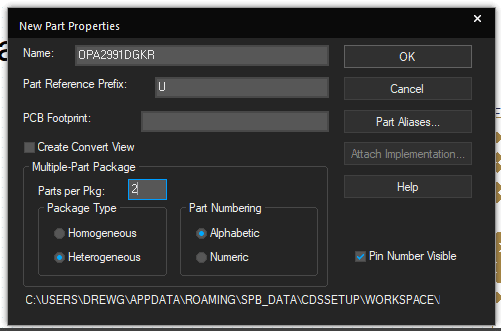
Users can set up Parts in separate sections using the Multiple-Part Package section.
-
Design the schematic symbol using standard component shapes and the manufacturer’s pin number/naming. Note the “A” following the schematic symbol – part numbering can be alphabetical or numeric but defaults to alphabetical.
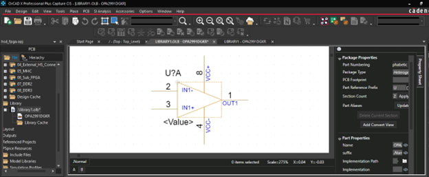
Designing the first section of a dual-channel op-amp. -
When done with the first section of the component, locate the dropdown below the bottom-left corner of the design canvas. Note that the schematic symbol increments either alphabetically or numerically. Select the next section of the part and design the remaining pins accordingly.
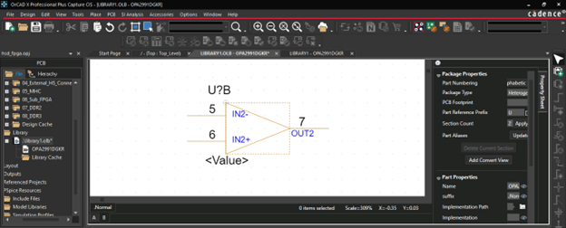
Designing the second section of a dual-channel op-amp. -
Repeat step 4 until all the sections of the part are complete. The part is now ready for placement in the schematic. To check for accuracy, users can navigate to “View” > “Package” from the top navbar to see all sections of the part side-by-side in a single window.
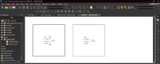
The Package window shows all sections of a Multiple-Part Package side-by-side. -
When placing the part, the designer will place the sections alphabetically (or numerically) until all the sections are in the schematic. Designers can cycle between different schematic pages to organize the circuit as desired.
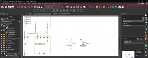
When placing Multiple-Part Packages, users will place one section at a time until complete.
Cadence Solutions for Schematic Design
Knowing how to put pins in sections using OrCAD X is invaluable when adding components with large pinouts or repeated circuit blocks. Designing parts this way allows schematic pages to remain uncluttered and translate easily to a board layout with a similar grouping arrangement. Multiple-part packages are just the tip of the iceberg regarding OrCAD X schematic design capabilities. Interested in learning more? See how Cadence PCB Design and Analysis Software simplifies all phases of ECAD design for quick turnaround times to meet tight deadlines.
Leading electronics providers rely on Cadence products to optimize power, space, and energy needs for a wide variety of market applications. To learn more about our innovative solutions, talk to our team of experts or subscribe to our YouTube channel.