Discussion of the MOSFET Simulation Model: Theory to Reality
Key Takeaways
-
Accurate MOSFET models require defining electrical parameters like threshold voltage, on-resistance, and transconductance.
-
Simulations should include switching behavior, parasitic elements, and body diode effects to reflect real performance.
-
PSpice simplifies MOSFET modeling with guided tools that turn datasheet values into simulation-ready components.

The adaptable and reliable MOSFET requires consideration in the design stage
MOSFETs (Metal-Oxide-Semiconductor Field-Effect Transistors) are building blocks in analog and digital circuits. Unlike bipolar transistors, MOSFETs are controlled by voltage at the gate, not current, making them highly efficient for switching and amplification. MOSFETs are transconductance devices at their core, meaning the input voltage controls the output current. This relationship, defined as
gm = ΔId / ΔVgs,
is central to the operation of MOSFETs in various applications.
From switching regulators to amplifiers, it is crucial to understand how MOSFETs behave across their different operating regions (cutoff, linear/ohmic, and saturation). This guide breaks down key characteristics and shows how to model MOSFETs accurately using PSpice, ensuring simulations align with real-world performance.
An Introduction to MOSFET Operation
Every MOSFET has drain, source, and gate electrodes. Rather than relying on current to operate, a MOSFET uses the gate voltage to change conductivity and cause switching or amplification. As a result, MOSFETs function as transconductance devices, i.e., devices that operate through a direct relationship between the input voltage and the output current. We can view this relationship as transconductance (gm) equaling the ratio of current change (iout) at the output to the voltage change at the input (vin), or:
gm = iout/vin
With MOSFETs, transconductance equals the change in the drain current divided by a slight change in the gate/source voltage with a constant drain/source voltage. Because of its interaction with the bias point, transconductance also functions as the gain parameter of MOSFETs. A transconductance amplifier has an output current proportional to its input voltage. As a result, the amplifier becomes a voltage-controlled current source.
MOSFET Internal Structure and Electrical Behavior
|
Aspect |
Description |
|
Channel Formation |
Built using ion implantation to create a conductive path between the source and drain under the gate. |
|
Threshold Voltage Polarity |
PMOS: Positive threshold voltage NMOS: Negative threshold voltage |
|
Carrier Movement & Threshold |
Electrons or holes enter at the source and exit at the drain. More carriers lower the threshold voltage (Vgs_th). |
|
Gate Insulation |
The metal oxide layer insulates the gate from the channel, forming a capacitor and enabling high input resistance. |
|
Gate Voltage Effect |
With no gate voltage, the channel exists but is not conducting. Applying a gate voltage modifies channel width and conductivity. |
MOSFETs have interesting characteristics that allow the devices to work in analog circuits as linear small signal amplifiers and digital circuits as switches. Given the high input impedance seen with MOSFETs, low or high-impedance sources can drive a MOSFET without degrading the signal. Along with having a high input impedance, MOSFETs have an extremely low drain-to-source resistance (Rds). Because of the low Rds, MOSFETs also have low drain-to-source saturation voltages (Vds), allowing the devices to function as switches.
Types of MOSFET Operating Modes
Manufacturers create the conductive channel in a MOSFET using ion implantation between the source and drain beneath the gate. This channel carries charge carriers that influence the threshold voltage polarity: PMOS devices have a positive threshold voltage, while NMOS devices have a negative one. The number of carriers affects the threshold voltage value—more carriers result in a lower threshold.
MOSFETs are depletion or enhancement types, which behave differently at zero gate-to-source voltage (Vgs).
|
Depletion-mode MOSFETs usually turn on and off when Vgs passes a threshold. In contrast, enhancement-mode MOSFETs are generally off and require Vgs to exceed a minimum level to conduct. For enhancement MOSFETs, the drain current depends on the gate voltage. |
Enhancement-mode MOSFETs operate in three regions based on Vgs and Vds values:
-
Ohmic (linear) region: device acts like a voltage-controlled resistor,
-
Saturation region: device functions as a constant current source,
-
Cut-off region: device is off and non-conductive.
Enhancement MOSFET Operation Modes
|
Ohmic Region |
Saturation Region |
Cut-off Region |
|
Vgs > Vthreshold Vds < Vgs |
Vgs > V threshold Vds > Vgs Id = Maximum value |
Vgs < Vthreshold Vgs < Vthreshold Id - 0 |
|
Voltage-controlled resistance |
Constant current – Transistor fully on |
Transistor fully off |
|
Amount of Vgs determines the resistive value Response is linear |
Closed switch Maximum current for the Voltage (Vgs) |
Open switch |
A quick study of the table shows how MOSFETs work as analog amplifiers and digital switches. Since increasing the gate to source voltage (Vgs) results in a corresponding increase in drain current (Id), enhancement mode MOSFETs can operate as amplifiers by controlling the output current in response to small changes in input voltage.
-
With a high input resistance, very little or no current flows into the gate.
-
As a result, current flows through the central channel between the drain and source.
-
The MOSFET functions as a voltage-controlled resistor, with the amount of current directly proportional to the input voltage. With the correct DC bias, a MOSFET amplifier operates in the linear region with a small signal superimposed over the DC bias voltage applied at the gate.
MOSFETs used for switching have a lower on-resistance rating and can carry greater amounts of current. Depletion-mode MOSFETs can handle higher voltages than enhancement-mode MOSFETs and can operate faster because of lower input and output capacitance.
Achieving Quiescence with MOSFETs
When we study electronics, we find that every transistor has a quiescent or Q-point at bias. Quiescence occurs when the AC signal equals zero or has gone quiet, and only the DC biasing values remain. At the Q-point, we see a steady-state DC voltage or current at a specific terminal with no applied input signal.
When a MOSFET functions as an amplifier, the device's transconductance is a Q-point function. The transconductance (gm) is the slope of the line tangent to the active curve at the operating Q-point. An additional twist happens here because MOSFETs have forward transconductance (gfs). This forward transconductance becomes defined by a change in drain current divided by the change in gate-to-source voltage at a Q-point, with the drain-to-source voltage (Vds) remaining constant. The forward transconductance value varies with the curve's Q point. Any change in the Q-point changes the slope of the tangent line.
Simulation for MOSFETs and Electronics With MOSFETs
Using SPICE simulation with MOSFETs can ensure that your design will perform accurately with current and voltage calculations and without pesky parasitics. PSpice contains an over 34,000-model library with specific MOSFET parameters and an easy and intuitive parameter editing system to adjust for gain and Q-point necessities.
How to Work With a MOSFET Simulation Model
Simulating a MOSFET requires a thorough understanding of its operating parameters and conditions. This approach involves understanding how the model reflects real-world electrical characteristics related to voltage, current, various operating regions, and environmental influences.
Static (DC) Characteristics and Key Model Parameters
|
Term |
What It Is |
How Simulations Help |
|
Gate-to-Source Threshold Voltage (Vgs_th) |
Minimum gate voltage required for the MOSFET to begin conducting; defines turn-on conditions and logic levels. |
Use a DC Sweep of Vgs while monitoring ID to verify accurate turn-on behavior. This ensures switching occurs at the correct voltage. |
|
Drain Current (Idss) |
Maximum drain current that flows when the gate to source voltage (Vgs) is zero and the device is operating in the saturation region - typically applicable to depletion mode MOSFETs. |
Use DC Sweeps to plot transfer (Id vs. Vgs) and output (Id vs. Vds) characteristics to validate current behavior under different biasing conditions. |
|
On-Resistance (Rds_on) |
Resistance when the MOSFET is fully on impacts power loss and efficiency in switching. |
Simulate at the intended Vgs to confirm the Rds_on matches expectations under typical operating conditions. |
|
Transconductance (gm) |
A measure of how well the gate voltage controls the drain current (gm = ΔId/ΔVgs); crucial for analog gain. |
Observe the slope of Id vs. Vgs in the saturation region using DC Sweep or AC analysis to extract and validate gm. |
|
Breakdown Voltages (Vds_max, Vgs_max) |
The maximum voltage the device can safely handle without damage. |
Use Smoke Analysis or define limits in simulation to detect violations. Confirm your testbench never exceeds datasheet-rated breakdown voltages. |
Dynamic Switching Behavior
Beyond static behavior, analyzing the dynamic switching characteristics of a MOSFET is helpful for many applications. The inter-electrode gate capacitances (Cgs, Cgd, Ciss, Coss, Crss) are fundamental in determining:
-
Switching speed
-
Gate drive requirements (related to Gate Charge, Qg)
-
Overall noise susceptibility
To accurately model these capacitances, run a Transient Analysis with realistic gate drive signals, accounting for driver output impedance and any series gate resistance. This setup enables precise observation and measurement of turn-on/turn-off time and propagation delays. An inadequate gate drive current can cause the MOSFET to linger in the linear region during switching, increasing thermal stress.
Many discrete MOSFETs also include an intrinsic body diode. Key parameters to evaluate are:
-
Forward voltage drop
-
Reverse recovery time (trr)
-
Reverse recovery charge (Qrr)
These characteristics can significantly impact efficiency and cause problems in topologies like bridge converters, where the body diode may conduct.
Finally, evaluate switching losses by monitoring power dissipation (P = Id × Vds) during switching transitions within a transient analysis. This process is essential for selecting appropriate power MOSFETs and ensuring robust thermal design.
Realistic Operating Conditions
To truly reflect real-world performance, simulations must also account for realistic operating conditions, the impact of parasitics, and temperature effects. Board-level parasitics like lead inductance and trace capacitance can introduce ringing or slow switching. In simulation, these can be represented by adding discrete L/C components in the simulation schematic or by using advanced package models.
MOSFET parameters such as Vgs_th and Rds_on are Temperature-Dependent. As such, PSpice supports temperature-dependent modeling, and performing temperature sweep simulation is vital for verifying robust operation across the intended environmental range, especially given potential humidity or thermal stress.
How to Create a MOSFET Simulation Model with PSpice
PSpice offers a wizard-like tool called the Modeling Application to simulate common device types like a MOSFET. This tool provides a guided approach to creating custom PSpice models based on key datasheet parameters without needing to delve directly into the complexities of SPICE netlist syntax. Let's walk through creating a P-channel MOSFET model as an example.
Step 1: Open the Modeling Application
Within PSpice , navigate to the menu and select Place > PSpice Part > Modeling Application.
Step 2: Select Device Type
A panel will appear, offering choices for the type of model you wish to create. For our P-channel MOSFET, we first select "Power MOSFET" from the categories, and then select "P-Channel MOSFET."
Step 3: Enter Datasheet Parameters
The application will present a series of fields corresponding to key electrical characteristics. You can modify these values based on the specific MOSFET datasheet you are working from.
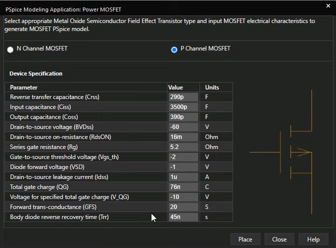
Step 4: Place the Component
After entering all known parameters, click the "Place" button. The Modeling Application will generate the PSpice model and an associated schematic symbol. You can then click on your schematic to place the newly created component. Use keyboard shortcuts like 'V' to flip vertically or 'H' to flip horizontally if needed. Models created this way are immediately ready for simulation within the current design.
Building an accurate MOSFET simulation model ensures that your design matches real-world environments. Designers can easily define and simulate complex MOSFET behavior using the PSpice Modeling Application—no SPICE coding is needed. Get started with PSpice through the OrCAD X Free Trial. Or explore the full capabilities of the OrCAD X platform to elevate your next power or analog design.
Leading electronics providers rely on Cadence products to optimize power, space, and energy needs for a wide variety of market applications. To learn more about our innovative solutions, subscribe to our newsletter or our YouTube channel.