Does HDI Improve Signal Integrity? The Real Electromagnetic Impact of Microvias
The conventional wisdom holds that high-density interconnect (HDI) design improves signal integrity: shorter interconnects, smaller vias, reduced parasitic capacitance and inductance. This idea is mostly accurate, but it oversimplifies reality and doesn’t account for nuance. Understanding when and why HDI helps signal integrity, and recognizing the scenarios where it can actually introduce new challenges, is essential for making informed design decisions.
Via Stub Behavior: HDI vs. Through-Vias
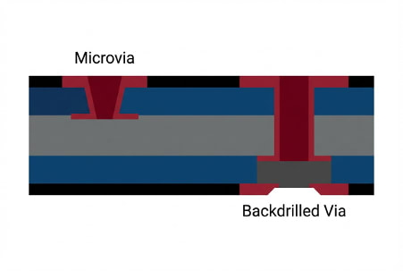
Figure 1: Microvia (no stub) vs. Through-via stub with backdrill cross-section
Via stubs are among the most significant signal integrity impairments in high-speed design. When a through-via connects a signal on layer 1 to a trace on layer 4 of an 8-layer board, the unused portion of the via extending from layer 4 to layer 8 acts as a resonant stub. Energy couples into this stub and reflects back toward the source, creating frequency-dependent insertion loss notches that can devastate multi-gigabit signaling.
The stub resonance frequency depends on stub length. A 60-mil stub in FR-4 (Er≈4) resonates around 12.3 GHz at the quarter-wave frequency, placing the first null squarely within the bandwidth of 10+ Gbps serial links. Backdrilling removes stub material but adds manufacturing cost and complexity.
Microvias eliminate this problem by design. A microvia connects only adjacent layers, meaning, there is no stub. The signal energy that enters the via exits entirely on the target layer with no resonant structure to create reflections.
This advantage compounds with frequency. At 5 Gbps, via stubs are problematic but manageable. At 25 Gbps and beyond, stub elimination becomes essential, making HDI the natural choice for the highest-speed interfaces.
Effects on Differential Skew and Jitter
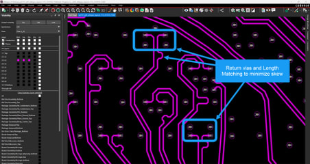
Figure 2: Matched positive and negative via placement from NVIDIA AGX Orin PCB layout (Credit: HaSofu , screenshot)
Differential signaling depends on balanced propagation between the positive and negative legs of a pair. Skew is the timing difference between traces that need to synchronize their information (e.g. D+ and D- on a differential pair or D0 – D7 on a data lane in a DDR chip). The timing difference, or skew, directly impacts eye opening and jitter. Via transitions are common sources of skew because manufacturing tolerances, routing asymmetries, and via placement variations can create path length differences between P and N signals.
HDI offers both advantages and potential pitfalls for differential skew management.
On the positive side, microvias enable tighter via-to-via spacing than through-holes because their smaller pad sizes consume less routing real estate. Closer P/N vias minimize the length difference that asymmetric via placement creates.
Microvias also transition signals between layers over shorter vertical distances, reducing the propagation time through the via structure itself. In through-via designs, the vertical propagation time through a 62-mil board can contribute measurable skew if P and N vias have different stub lengths or reference plane connections.
The potential pitfall lies in sequential via transitions. If a differential pair requires multiple layer transitions using stacked or staggered microvias, each transition must be carefully matched between P and N. Asymmetric via stacking where P uses a two-level stack but N requires a three-level stack to reach the same destination creates a skew that accumulates across the channel.
Successful HDI design for differential signaling requires explicit attention to via structure symmetry, planning layer transitions so both legs traverse identical via stacks.
Reference Plane Considerations
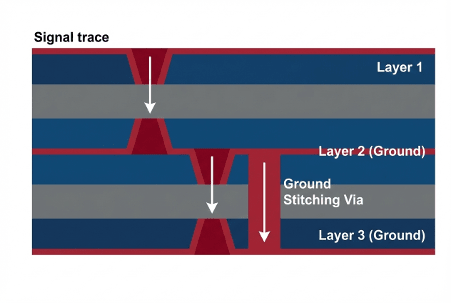
Figure 3: Layer transition without ground stitching via (upper left) vs with ground stitching via (lower right)
Every high-speed signal requires a reference plane to establish controlled impedance and carry return current. The relationship between signals and references in HDI designs differs from conventional designs in important ways.
HDI stackups often use very thin dielectrics—2 to 4 mils—between buildup layers. These thin dielectrics provide tight coupling between signal and reference, which improves impedance control and reduces crosstalk between adjacent traces. The higher distributed capacitance also benefits power integrity by lowering plane-pair impedance.
However, thin dielectrics require narrower traces to achieve target impedances. A 50-ohm microstrip on a 4-mil dielectric might require a 3-mil trace, pushing toward the edge of standard fabrication capabilities. This trace-width reduction must be balanced against current-carrying requirements and manufacturing yield.
Reference plane continuity also demands more attention in HDI designs. Because microvias only connect adjacent layers, a signal transitioning from layer 1 to layer 3 via two stacked microvias may change references twice—from the layer-2 plane to the layer-3 plane. Each reference change requires ground stitching to maintain return-path integrity. Designs that neglect this stitching exhibit degraded signal integrity despite using HDI structures.
When Microvias Reduce vs. Increase Loss
The loss characteristics of microvia transitions are generally favorable but not universally so.
Microvias reduce loss when: They eliminate stubs that would otherwise create resonant loss. They shorten vertical interconnect distances, reducing resistive and skin-effect losses through the via barrel. They enable shorter horizontal routing by providing layer transitions closer to source and destination.
Microvias may increase loss when: Multiple stacked or staggered transitions replace a single through-via connection, accumulating transition losses. The smaller via diameter increases resistance compared to larger through-vias, which becomes significant at high current densities. Poor fill quality introduces voids that create impedance discontinuities and reflective losses.
The net effect depends on the specific design. For signals that would otherwise suffer significant stub resonance, HDI almost always wins. For signals that could route effectively on two layers with clean through-via transitions, the calculus is less clear, and forcing HDI for its own sake may not improve performance.
The Bottom Line
HDI genuinely improves signal integrity in most high-frequency applications, but it does so through specific mechanisms;primarily stub elimination and reduced interconnect length, rather than through any magical property of microvias themselves.
Realizing these benefits requires deliberate design practices: maintaining via structure symmetry for differential pairs, explicitly managing reference transitions with ground stitching, and matching dielectric thickness to trace geometry for impedance control.
Designers who understand the electromagnetic mechanisms at work can leverage HDI to achieve signal integrity performance that conventional approaches cannot match. Those who adopt HDI without this understanding may find that the technology delivers less than promised or introduces new problems to replace the old ones.