Understanding Power Supply Topologies: From Buck to LLC Resonant
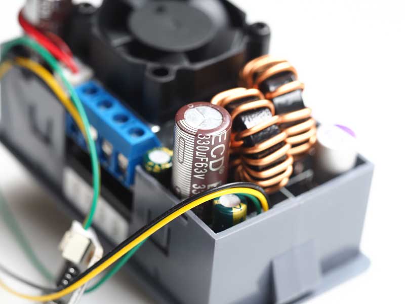
Power Converter
Key Takeaways
Here is a TLDR cheat sheet for understanding power supplies:
• You can quickly tell which power supply is which based on these three:
-
- Isolated vs. non-isolated
- Voltage range
- Power level in Watts
• For step-down, use the Buck converter. For increasing voltage (e.g. from 9 V to 12 V) use the boost converter. For when your output voltage can go lower or higher than input voltage, use a Buck-Boost converter.
• For any designs requiring 150 Watts or under, you'll likely use a Flyback converter. Especially if it's isolated (typical for wall plugs and power supplies for consumer electronics)
• Use SPICE simulation to verify your switched-mode power converters work, especially if you have manufacturer SPICE models. Simulation has saved me many times.
Why Topology Choice Matters in Power Supply Design
Every power supply designer has this question at the beginning: Do I use a buck, boost, flyback, forward, or something else? Is there much difference?
Each topology operates in a different way, and understanding how each one works is essential before making a choice.
This article provides a practical way to choose power supplies found in real products. Over time, you may go from basic switched-mode converters to advanced topologies like multi-rail, higher-power systems.
Non-Isolated Power Supply Topologies
When to Use a Buck Converter
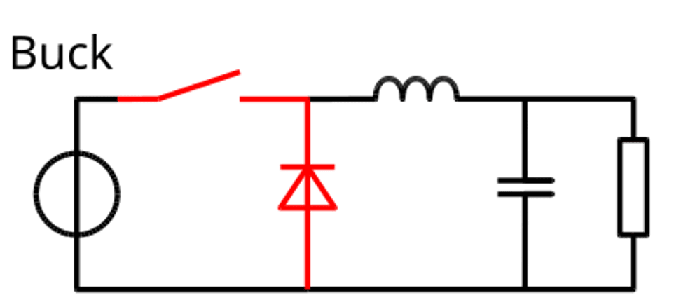
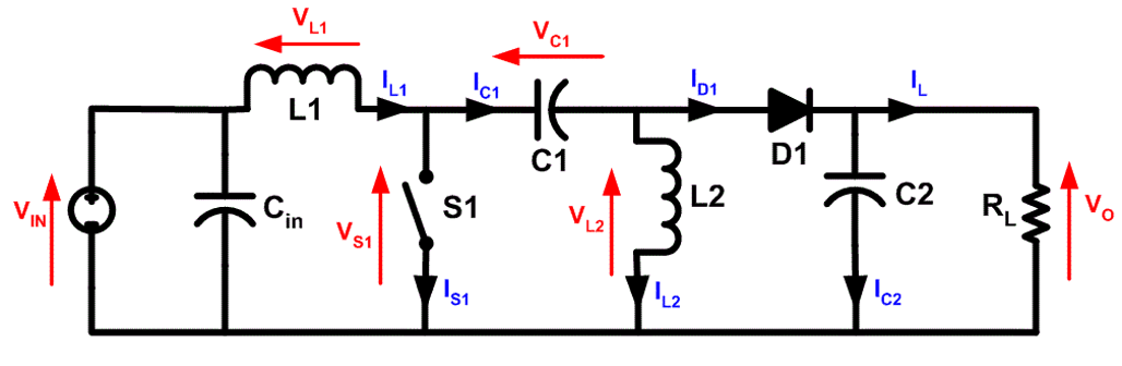
A buck converter is the go-to choice when your output voltage is significantly lower than your input voltage, specifically, by more than 33%. This threshold is important because, for smaller voltage drops, a linear dropout regulator (LDO) can achieve the same result. However, when the input voltage is much higher than the output, LDOs generate excessive heat, making them inefficient for such applications. For example, if you're stepping down from 24V to 5V, a buck converter is far more efficient than an LDO. Buck converters are typically used in applications where the current ranges from hundreds of milliamps to tens of amps, and isolation is not required.
Engineers favor buck converters for several reasons. They are simple, well-understood, and supported by a vast ecosystem of controllers and modules. When designed correctly, they can achieve high efficiency, often exceeding 90%. Additionally, their small magnetics make them ideal for moderate step-down ratios, and poly-phase variants allow them to scale to very high power levels, making them versatile for a wide range of applications.
However, there are some challenges to watch out for when using buck converters. Layout-driven electromagnetic interference (EMI) can be a significant issue, particularly due to hot loops and switch node ringing. The input current is always discontinuous, which can lead to higher conducted EMI. Additionally, duty-cycle constraints can arise when stepping down from very high to very low voltages, potentially pushing the limits of minimum on-time. Fortunately, EMI issues can be mitigated with the use of filter components such as chip beads, common mode chokes, and filter chokes, ensuring a cleaner and more reliable design.
For medium-sized organizations with growing product lines, bucks usually power local point-of-load rails: digital core voltages, IO rails, sensor supplies, etc.
When to Use a Boost Converter
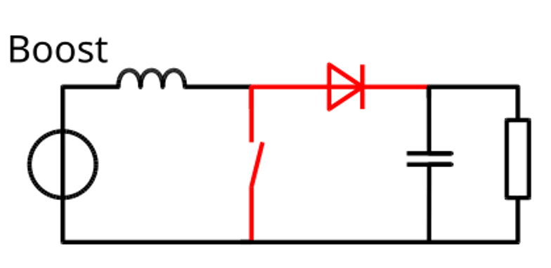
A boost converter is the ideal choice when your input voltage is consistently lower than your output voltage. For example, if you need to step up from 5V to 12V for an LED rail, a boost converter is the ideal solution. It's particularly useful in applications where you're running from a battery or a low-voltage bus but still need to achieve higher voltage rails. Additionally, boost converters are suitable for scenarios where isolation is not required, making them a straightforward and efficient solution for many designs.
Boost converters are commonly found in applications such as LED drivers, audio amplifiers, and certain sensor rails. They are also widely used in battery-powered industrial or IoT devices that require "above-battery" voltage levels. Another key use case is in Power Factor Correction (PFC) circuits, where the boost converter's ability to draw current continuously in continuous conduction mode makes it an excellent choice for improving power quality and efficiency.
However, boost converters come with their own set of challenges. One major pitfall is the risk of output short circuits, which can cause significant damage if not properly protected. Additionally, electromagnetic interference (EMI) can be more problematic compared to buck converters, as the input experiences pulsed current. Another consideration is the control loop behavior, which can change dramatically as the duty cycle increases, requiring careful design and tuning to ensure stable operation.
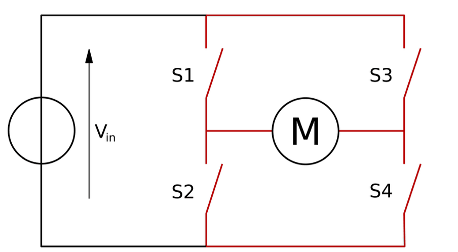
When to Use a Buck-boost / inverting Converter
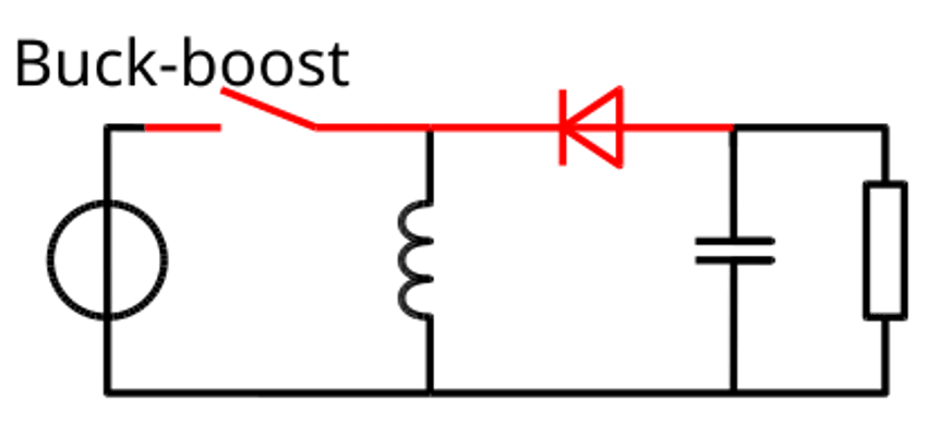
Buck-boost Converter (Wikipedia)
A buck-boost converter (non-isolated) is the ideal choice when your input voltage falls into an overlap zone where it can sometimes be higher than the output voltage (VIN > VOUT) and other times lower (VIN < VOUT). For example, if your input voltage ranges from 2.7V to 5.5V but your output needs to remain at 3.3V, a buck-boost converter is the perfect solution. Additionally, if you need to generate a negative rail from a positive input, an inverting buck-boost converter is the go-to option.
Buck-boost converters are commonly used in battery-powered systems, especially as the battery discharges and the input voltage fluctuates. They are also valuable in mixed-signal systems where a small negative rail is required for components like operational amplifiers (op-amps) or analog-to-digital converters (ADCs). These use cases highlight the versatility of buck-boost converters in handling dynamic voltage requirements.
However, there are important considerations to keep in mind when using a buck-boost converter. The control and MOSFET arrangement are more complex compared to straightforward buck or boost converters, requiring careful design. Efficiency and ripple tradeoffs also demand thorough simulation to ensure optimal performance. Additionally, the layout is more sensitive to current loops and parasitics, which can impact stability and efficiency. One key challenge is that the output polarity is inverted, which can complicate system design. Furthermore, the switch lacks a ground reference, making the drive circuit more complex to implement. These factors make buck-boost converters powerful but require meticulous attention to detail during the design process.
When to Use a Single-Ended Primary-Inductor Converter (SEPIC)
Single-Ended Primary Inductor Converter (SEPIC) (Wikipedia)
The SEPIC addresses one of the biggest challenges of the buck-boost converter: inverted output polarity. By design, the SEPIC provides a non-inverted output, making it a preferred choice in applications where maintaining the same polarity as the input is critical. This makes it particularly useful when the input voltage crosses the output voltage, similar to a buck-boost scenario, but without the complication of inverting the output. SEPIC is also ideal for battery-powered applications where the voltage may sag below nominal levels, yet a regulated output is still required.
The SEPIC topology differs from the buck-boost in several key ways. It uses two inductors (or a single coupled inductor) along with a coupling capacitor. This coupling capacitor not only helps achieve a non-inverted output but also provides some limited isolation, which can be advantageous in certain designs. While the SEPIC is more complex than a buck-boost converter, it effectively eliminates the polarity issue, making it a practical solution for specific use cases.
For SEPIC designs, catalog coupled inductors are readily available, and custom inductors can be sourced for specialized needs. Additionally, the related Ćuk topology offers similar benefits but with an inverted output, providing another option for engineers depending on their design requirements. While SEPIC's added complexity may require more careful design and simulation, its ability to deliver a non-inverted output makes it a valuable tool in power supply design.
Isolated Power Supply Topologies
When safety standards or system architecture demand galvanic isolation, you move into transformer-based topologies. The choice depends primarily on power level, output current requirements, and efficiency targets.
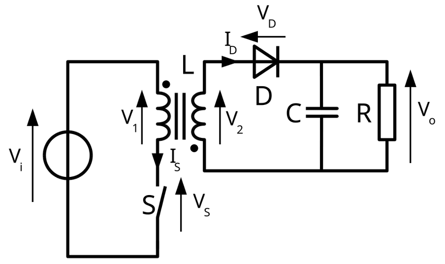
When to Use a Flyback converter
Flyback Converter (Wikipedia)
The flyback converter is the ideal choice when isolation is required, such as in applications where mains power needs to be stepped down to low-voltage outputs. It is well-suited for power levels ranging from just a few watts up to approximately 150W. Flyback converters can support one or more outputs with different voltage levels, making them versatile for multi-output designs. However, they are best used for output currents below 10A, as the high peak currents inherent to flyback operation make them unsuitable for high-current applications.
Flyback converters are commonly found in a variety of applications, including phone chargers and USB-C power adapters, industrial IO modules and PLCs, LED drivers, and auxiliary power rails in larger systems. Their widespread use is a testament to their versatility and efficiency in these scenarios.
Engineers continue to choose flyback converters for several reasons. A single magnetic component, a transformer, can provide multiple isolated rails, simplifying the design. The structure is straightforward, as no separate output inductor is needed; the transformer itself serves as the storage inductor. Flybacks are also cost-effective for mid-power designs and are particularly well-suited for high-output voltages, making them a practical choice for many applications.
However, flyback converters come with tradeoffs. Magnetics design is critical, requiring careful attention to core selection, turns ratio, air gap, and leakage inductance. The transformer must include an air gap to store energy, which adds complexity to the design. Additionally, peak currents and switching stress are higher than in some other topologies, which can lead to challenges with electromagnetic interference (EMI). Proper design of snubbers, RCD clamps, and layout is essential to mitigate these issues. Finally, flybacks are not suitable for output currents above 10A; for such applications, forward converters are a better option.
For medium-sized companies scaling up, flyback converters often represent the first significant step into isolated power designs. This is where process maturity, documentation, and simulation tools become critical to ensure the design is robust and ready for production.
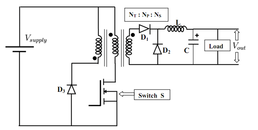
When to Use Forward converter
Forward Converter (Wikipedia)
The forward converter is essentially a transformer-isolated version of a buck converter, designed to address one of the flyback converter's main limitations: its inability to handle high-current outputs. Forward converters are ideal when isolation is required, the output current exceeds 10-15A, and the power levels range from approximately 20W to 200W. These characteristics make forward converters a reliable choice for applications demanding higher current capabilities.
The key difference between flyback and forward converters lies in how energy is stored and transferred. In a flyback converter, the coupled inductors themselves store energy, which requires an air gap in the core that 'combines' them into a pseudo transformer. In contrast, a forward converter does not store energy in the transformer. Instead, it uses a separate output inductor, also known as a storage choke, to store energy. This design eliminates the need for an air gap in the transformer but adds an extra component to the circuit.
Forward converters excel in high-current applications because the output current is non-pulsating, thanks to the filtering provided by the output inductor. This makes them far better suited for handling currents above 15A compared to flyback converters. However, this advantage comes with tradeoffs. The addition of an output inductor increases the part count and makes the design slightly more complex. Forward converters are also less suitable for high-voltage outputs, where flyback converters perform better. Additionally, core reset requirements in forward converters add another layer of complexity to the design process.
Despite these challenges, forward converters remain a popular choice for high-current, isolated power supply designs, offering a balance of performance and reliability for demanding applications.
When to Use Push-pull converter
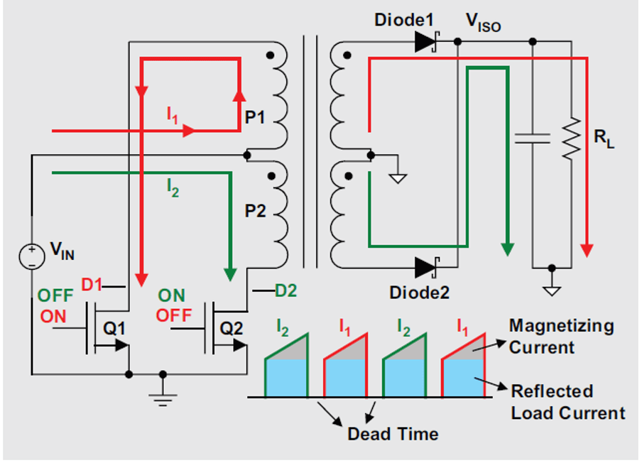
Push-pull Current Paths Waveforms. Source: Texas Instruments
The push-pull topology is essentially an advanced version of a forward converter, featuring two primary windings that create a dual-drive winding. This design allows the transformer core to be utilized much more efficiently compared to flyback or standard forward converters, making it a powerful option for certain applications.
One of the key advantages of the push-pull topology is its ability to scale to higher power levels than both flyback and forward converters. Additionally, it offers better core utilization, which improves overall efficiency. At similar power levels, push-pull designs also require smaller filters compared to forward converters, which can simplify the design and reduce component size.
However, the push-pull topology comes with critical concerns that must be carefully managed. One major risk is shoot-through, which occurs if both switches are turned on simultaneously. This creates equal and opposite flux in the transformer, resulting in low impedance and potentially destructive shoot-through currents. Another challenge is the high switch stress, which can reach 2×VIN. This makes the topology less suitable for applications involving 250VAC input or power factor correction (PFC). Additionally, only half of the transformer's copper is used at any given time, which increases copper losses and reduces efficiency.
Despite these challenges, the push-pull topology remains a valuable option for designs requiring higher power levels and efficient core utilization, provided the risks are mitigated through careful design and control.
When to Use a Half-bridge converter
Half-Bridge Converter (Wikipedia)
The half-bridge topology is a versatile design that scales well to higher power levels and is built on the foundation of the forward converter topology. One of its key advantages over the push-pull topology is reduced switch stress. In a half-bridge design, the switch stress equals the input voltage (VIN), unlike push-pull converters where the stress is 2×VIN. This makes the half-bridge topology a more reliable choice for certain high-power applications.
The half-bridge topology is particularly suitable for scenarios involving 250VAC input or power factor correction (PFC) applications, where the higher switch stress of push-pull designs becomes a limitation. It is also ideal for power levels ranging from 100W to 500W, especially in cases where efficiency and electromagnetic interference (EMI) are more critical than simplicity. These characteristics make it a popular choice for medium- to high-power designs.
However, the half-bridge topology comes with its own set of challenges. Like the push-pull topology, it is susceptible to shoot-through, which occurs when both switches are turned on simultaneously. To prevent this, the design requires dead-time between switch transitions. This dead-time, however, limits the duty cycle to about 45%, which can constrain the design in certain applications. Additionally, while the half-bridge topology handles higher output currents than push-pull, it is less suited for very high-current outputs, which may require alternative topologies.
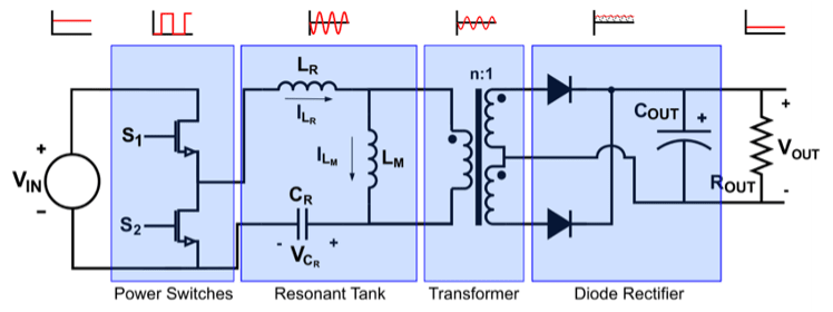
When to Use a LLC resonant converter

LLC Resonant Converter (Monolithic Power)
The LLC resonant topology is an advanced variation of the half-bridge converter that leverages resonant techniques to achieve zero-voltage switching (ZVS), even under no-load conditions. This capability significantly reduces switching losses, making the LLC resonant topology a highly efficient option for power supply designs.
LLC resonant converters are ideal for applications where high efficiency is critical, such as server power supplies and data center power systems. They are well-suited for power levels ranging from 200W to over 2kW and excel in scenarios requiring a wide input voltage range. Additionally, they are a great choice for power supplies that operate at high duty cycles, such as always-on applications. These features make the LLC resonant topology a dominant choice in high-power applications.
The popularity of LLC resonant converters in high-power designs is driven by several factors. Zero-voltage switching minimizes switching losses, enabling exceptional efficiency. The topology also scales effectively to very high power levels and is better suited than push-pull or standard half-bridge designs for handling wide input voltage ranges. As a result, modern desktop PC main power rails have largely transitioned to LLC resonant designs, further cementing its role in high-performance power supplies.
However, the LLC resonant topology comes with tradeoffs. Its complexity and cost are significantly higher than simpler topologies like flyback or forward converters. Additionally, the resonant tank circuit must remain energized continuously, making it less suitable for standby mode applications. Designing the resonant components also requires careful attention to detail, as improper design can compromise performance and efficiency.
LLC Resonant Converter (Monolithic Power)
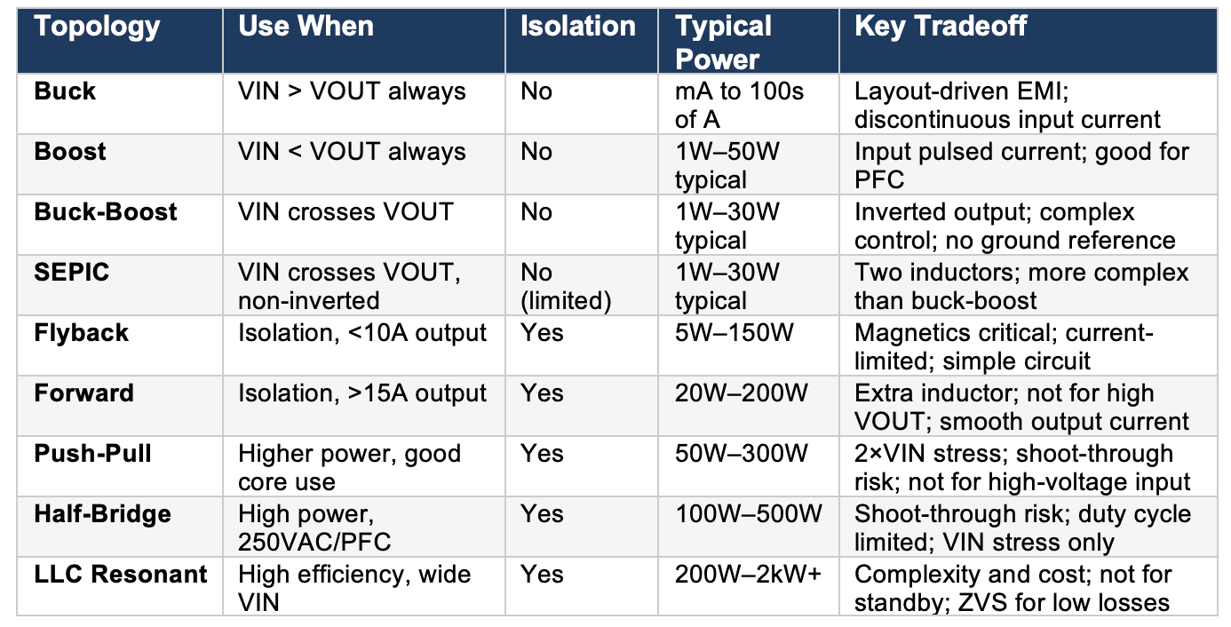
Quick Reference: Comparing Power Supply Topologies
 Power Level vs. Topology Range Chart - Horizontal bar chart showing approximate power ranges for each topology. Visual aid for quick topology selection based on power requirements.
A Simple Decision Flow in Your Head
You can implement this as a literal flowchart or keep it as a mental checklist:
1. Need isolation?
- Yes → Go to step 5.
- No → Go to step 2.
2. Is VIN always above VOUT?
- Yes → Start with buck.
- No → Go to step 3.
3. Is VIN always below VOUT?
- Yes → Start with boost.
- No → VIN crosses VOUT → Go to step 4.
4. Non-isolated, VIN crosses VOUT:
- Need non-inverted output? → SEPIC
- Inverted output OK? → Buck-boost
- Need negative rail? → Inverting buck-boost
5. Isolated topology selection:
- Power <150W AND output current <10A → Flyback
- Power <200W AND output current >15A → Forward
- Power 100-500W, high-voltage input → Half-bridge
- Power >200W, efficiency critical → LLC resonant
6. Special cases:
- Very high power density + narrow VIN/VOUT → Consider resonant/LLC or multi-phase bucks.
- Multiple isolated outputs → Flyback with multiple secondaries.
- Desktop PC main rail → LLC resonant (modern standard).
- Desktop PC standby rail → Flyback (always-on, low power).
After you pick a topology, you're not done-you've just constrained the design space so you can simulate and iterate intelligently. Your next step is validating efficiency across load points, checking switch stress under transients, and confirming thermal behavior before anyone spins a board.
Where Modern Tools Fit
Choosing a topology is only step one. Next, you want to validate that decision before anyone spins a board:
Use PSpice in Allegro X to:
- Compare efficiency across candidate topologies at different load points.
- Check switch stress and snubber needs under line and load transients.
- Visualize current waveforms in the magnetics and diodes before you pick parts.
- Validate resonant tank behavior for LLC designs.
Then, inside Allegro X layout, you can:
- Route switch loops to minimize EMI.
- Apply constraints for creepage/clearance on isolated designs.
- Hand off clean data to signal/power integrity tools as the architecture scales.
As part of this power supply campaign, we complement this article with a flyback-focused blog, a step-by-step design guide, and a webinar series that walks through PSpice simulation and Allegro X layout for real isolated supplies.
Together, these help engineers at growing companies move from "I think this topology works" to "we know this architecture will survive the lab and the field."
Resources
- Power Electronics Handbook (comprehensive reference)
- Texas Instruments Power Supply Design Seminars
- Cadence PSpice
- Manufacturer application notes (Some are better than textbooks for practical applications)
- Würth Elektronik Application Guides (topology-specific magnetics guidance)