Monitoring Standard PCB Trace Thickness and Width in OrCAD X
Key Takeaways
-
Copper thickness in PCBs is commonly measured in oz/ft², where 1 oz/ft² equals 35 µm or 1.38 mils, establishing a uniform thickness across boards.
-
The default trace thickness for most PCB designs is 1 oz/ft², but higher voltage or special requirements might necessitate thicker layers, with options ranging from 0.5 oz/ft² to 6 oz/ft².
-
Designers can use standards like IPC-2221 and various software tools or online calculators to determine the optimal trace dimensions based on current capacity, signal integrity, and thermal management needs.

OrCAD X makes routing with specified trace thicknesses simple
In the PCB industry, copper thickness is typically measured in ounces. This might seem odd since ounces are a unit of weight, not thickness. However, when 1 ounce (28.35 grams) of copper is spread evenly over one square foot of surface area, it forms a layer 1.37 mils (0.0348 mm) thick. This standard measurement helps maintain consistency across different PCBs.
Most commonly, PCBs are produced with a copper thickness of 1 oz (or 1 oz/ft2). In other words, without specific instructions in the design files, manufacturers usually assume a standard PCB trace thickness of 1 ounce for all layers. A thicker copper layer may be required for designs that need to withstand higher voltages or have specific resistance or impedance requirements. Various online calculators are available to assist in determining the necessary thickness, width, or length of traces to meet design specifications.
Default PCB Trace Thickness of Common PCB Manufacturers
|
Thickness (oz/ft²) |
Thickness (μm) |
Thickness (mils) |
|
0.5 |
17.5 |
0.69 |
|
1 (standard) |
35 |
1.38 |
|
2 |
70 |
2.76 |
|
3 |
105 |
4.13 |
PCB trace width, thickness, and length illustrated.
Alt-text: PCB trace width, thickness, and length illustrated.
PCB Trace Width vs. Thickness
When referring to a copper PCB trace, there are three main dimensions:
- Width
- Thickness
- Length
The designer determines the length as they route and subsequently determines things like impedance. You may see resources that refer to width and thickness interchangeably. In this article, the thickness specifically refers to the dimension perpendicular to the PCB plane. In other words, how far out of the board it measures.
The standard PCB trace thicknesses available from most PCB manufacturers start at 0.5 oz/ft² (approximately 17.5 µm) and typically go up to 2, with some options up to 6 oz/ft² (approximately 210 µm, although quite uncommon) or more for high current applications.
Calculating Trace Thickness
The IPC-2221 standard provides a comprehensive methodology to calculate the appropriate trace thickness. It considers the maximum current carrying capacity, allowable temperature rise, and ambient operating conditions. Software tools such as OrCAD X (discussed below) and online calculators are available to assist designers in applying these standards.
Factors Determining Trace Widths and Thickness
|
Factor |
Description |
|
Current Carrying Capacity |
Determines trace thickness based on the amount of current the trace must carry without significant heating. |
|
Signal Integrity |
Thicker traces reduce resistance and electromagnetic interference, which is crucial for maintaining the quality of high-frequency or sensitive analog signals. |
|
Thermal Management |
Thicker traces are better at dissipating heat, which is essential in high-power applications to prevent performance degradation. |
|
Mechanical Strength |
In environments with physical stress, thicker traces are less likely to break or wear, enhancing durability. |
Designers can choose any size for traces, provided they meet the minimum size and spacing requirements that the PCB manufacturer stipulates for a chosen price level. For multilayer PCBs, particularly those with more than two layers, it's important to use thicker traces on the inner layers. This is because heat disperses less efficiently from the inner layers compared to the outer layers. The choice of inner layer copper foil can vary among 0.5 ounces, 1 ounce, or 2 ounces.
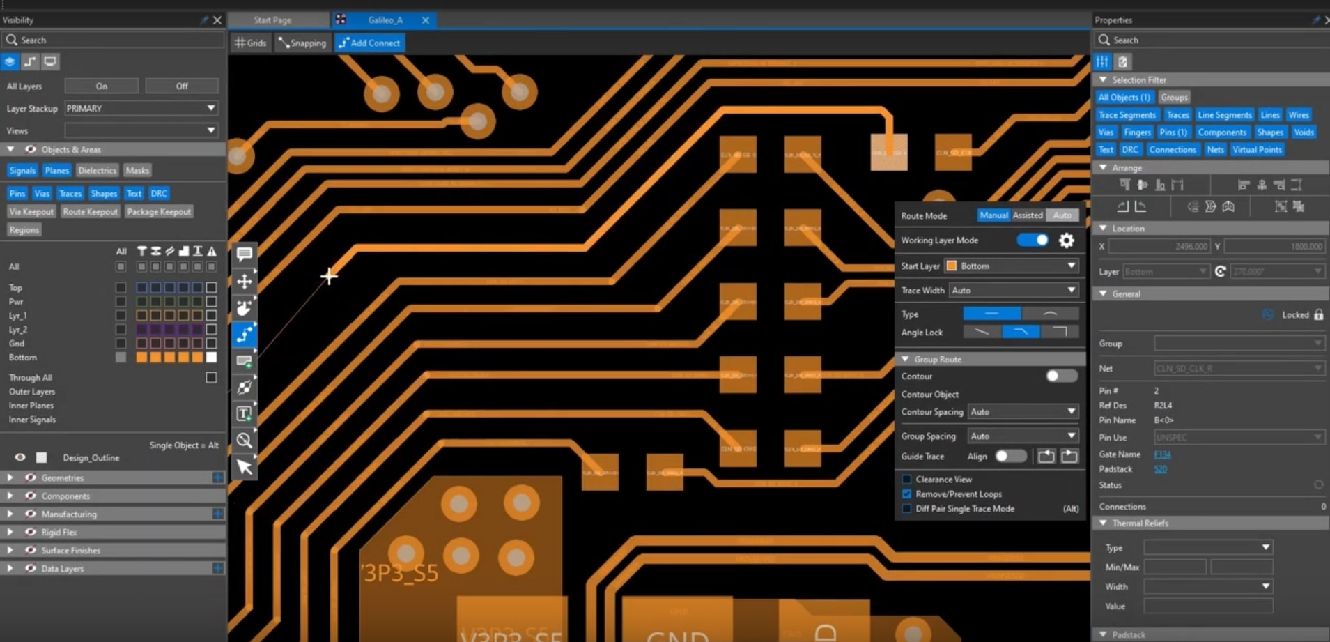
How OrCAD X Helps With Standard PCB Trace Thickness Monitoring
|
Feature |
Description |
Benefits for PCB Designers |
|
Interactive Routing and Trace Adjustment |
Enables the modification of trace dimensions using interactive tools and hotkeys. Users can switch between manual and assisted routing modes and dynamically adjust trace settings. |
Simplifies the process of setting trace thickness and width, allowing designers to make quick, precise adjustments that adhere to layout requirements and reduce potential rework. |
|
Designers can set specific constraints for trace widths and thicknesses, ensuring designs adhere to electrical performance and reliability standards. |
Ensures early in the design process that all traces meet specified electrical and physical requirements, preventing costly revisions during later stages of PCB development. |
|
|
Real-Time Constraint-Driven Feedback |
The Allegro-powered routing engine offers immediate feedback on constraint violations during routing, with tools like clearance view to highlight spacing issues. |
Allows for immediate corrections during routing, ensuring that the PCB meets design standards without the need for extensive troubleshooting in later phases. |
|
Visual Graphics for Routing |
Provides visual guides and via placement previews, enhancing the understanding of how traces interact with other PCB components, especially in complex routes. |
Assists in visualizing and planning trace layout, which is crucial for maintaining signal integrity and avoiding electromagnetic interference. This prevents errors before they occur. |
When working with a standard PCB trace thickness, ensure your designs meet industry standards without compromising efficiency with OrCAD X. OrCAD X streamlines your design process, from calculating trace dimensions to ensuring you meet industry standards. Discover OrCAD X now!
Leading electronics providers rely on Cadence products to optimize power, space, and energy needs for a wide variety of market applications. To learn more about our innovative solutions, talk to our team of experts or subscribe to our YouTube channel.