PCB Crosstalk Is a Layout Decision, Not a Post-Layout Issue
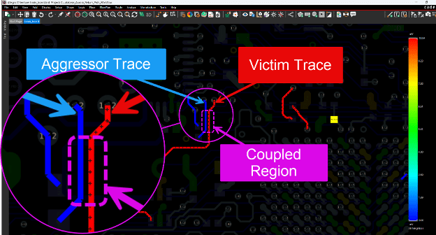
Figure 1. Crosstalk begins in the layout. Parallel routing and insufficient spacing create a direct coupling path between aggressor and victim traces, setting noise levels before the board is ever built.
A signal fails noise margin testing in the lab. You trace the noise back to an aggressor on the adjacent layer. The fix requires a re-route, and the schedule slips by a week.
This was avoidable. The spacing, the parallel run length, and the reference plane assignment were all known variables when the trace was drawn. The crosstalk that closed the noise margin was a direct result of those three choices.
Three PCB Design Decisions That Set Crosstalk Amplitude
Crosstalk amplitude is primarily determined by three layout variables. These are set during PCB design and not after fabrication.
Trace spacing. The electric and magnetic fields around a trace extend beyond the trace edges. A nearby trace sits inside those fields and picks up coupled energy . Wider spacing reduces the overlap. The reduction is not linear. Increasing spacing reduces both electric and magnetic field coupling, often producing a substantial reduction in induced noise voltage as field overlap decreases.
The working rule is three times the dielectric thickness between the trace and its reference plane, often called the 3H rule. The 3H guideline can reduce coupling significantly in many routing situations, but acceptable spacing ultimately depends on edge rate, routing topology, impedance requirements, and the allowable crosstalk budget for the interface. Tighter spacing is possible but needs to be checked, not assumed.
Coupled length. How far two traces run in parallel sets how much crosstalk accumulates. Far-end crosstalk (FEXT) grows with parallel length for the full run. Near-end crosstalk (NEXT) saturates after a certain length, which depends on the signal rise time. Short parallel segments keep both types of crosstalk small. Long parallel segments, especially in bus routing, are where crosstalk budgets quietly close.
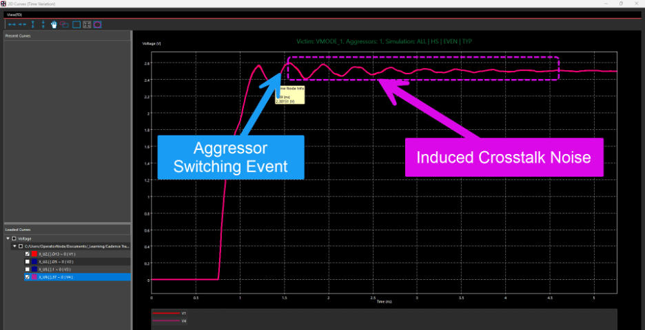
Figure 2. Crosstalk response measured on the victim net due to a nearby aggressor. The ringing and steady-state noise level are a direct result of the routed geometry, including spacing, coupled length, and reference plane quality.
Crossing adjacent layers at right angles is one way to keep the coupled length near zero. Routing orthogonally on neighboring signal layers is the layer-pair version of the same idea. Without a solid reference plane separating adjacent signal layers, broadside coupling can become stronger than same-layer edge coupling because the electromagnetic fields overlap vertically through the dielectric stackup.
Reference plane quality. A solid, continuous reference plane between two signal layers shields them from each other. If the reference plane has voids, splits, or antipad clearances that remove copper, the shielding weakens, and crosstalk between the two layers increases. A solid reference plane confines return current and terminates electric fields close to the signal trace. When plane continuity is degraded, the fields spread farther through the stackup, increasing coupling between nearby structures .
Why the Physics Matters
Understanding the physics behind crosstalk is essential for signal integrity in PCB design. Crosstalk originates from two mechanisms: mutual capacitance between conductors and mutual inductance between current paths. Both mechanisms scale with how much of the aggressor field reaches the victim.
Fast signal rise times contain high-frequency spectral content that strengthens capacitive and inductive coupling, allowing even relatively short routing segments to generate measurable crosstalk at modern edge rates.
Spacing controls that reach in the horizontal direction. Reference plane quality controls it in the vertical direction. Coupled length controls how long the victim sits inside the aggressor's field.
Change any of the three, and the crosstalk voltage at the victim receiver changes. This is not a tool artifact. It is the physics of coupled transmission lines. The tool just measures the result.
How to Reduce Crosstalk When Routing
The Impedance and Coupling workflow in Sigrity X Aurora reads the routed geometry and identifies which nets couple to which. The report lists aggressor-victim pairs and assigns each one a coupling coefficient. That coefficient tells you how tightly the two conductors talk to each other.
A crosstalk workflow can then estimate the induced noise on victim nets from nearby aggressors. In Sigrity X Aurora, coupling analysis identifies risky aggressor-victim relationships during layout, while more advanced crosstalk and eye-diagram simulations can be handled in the broader Sigrity X platform when required.
If the number is over budget, you open the layout, increase the spacing, shorten the parallel run, or improve the reference plane, and run the analysis again. The workflow is tight: find the problem, change the layout, confirm the fix.
Crosstalk as a Budget Line Item
High-speed interfaces run with a noise budget. Every noise source in the channel takes a piece of that budget. Power supply noise takes a piece. Intersymbol interference takes a piece. Crosstalk takes a piece.
If your crosstalk piece is bigger than the budget allows, the eye diagram closes and the bit error rate climbs. The fix is to shrink the crosstalk piece until the budget balances. That happens during routing, not after the board comes back.
The Layout Decision Frame
Crosstalk is not a post-layout issue . It is the direct outcome of layout decisions made during routing. You chose the spacing. You chose the coupled length. You chose the reference plane structure and layer assignment. Those choices determine how strongly the electromagnetic fields from one signal couple into another before the board is ever fabricated.
Measuring crosstalk during routing, instead of discovering it at test, costs zero extra board spins. It costs one afternoon of analysis. The math is simple.