PCB Power Integrity Analysis: Why PDN Behavior Is a Geometry Problem
A voltage regulator outputs 1.0 V. The integrated circuit (IC) needs 1.0 V within 3 percent. Somewhere between them, the voltage drops, or worse, the voltage rings.
The question is not whether the regulator works. The question is what the copper does to the power delivery path between the regulator and the IC.
Plane Pair Capacitance
When a power plane sits close to a ground plane, the two form a capacitor. The capacitance depends on three things: the area of overlap, the dielectric constant of the material between them, and the thickness of that dielectric.
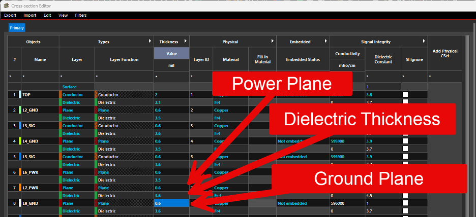
Figure 1: Adjacent power and ground planes form a distributed capacitor. Reducing dielectric thickness increases capacitance per unit area, extending PDN effectiveness into higher frequencies.
Thin dielectric means more capacitance per unit area. That capacitance works at frequencies where discrete decoupling capacitors run out of usefulness. A typical ceramic capacitor becomes inductive above a few hundred megahertz. Plane pair capacitance keeps working well past that point because the current path is short and wide instead of long and narrow.
The Cross-Section Editor in Allegro X PCB Layout sets this spacing for you. Place your power plane and ground plane on adjacent layers. Specify the dielectric thickness. That single decision, made early in the design, sets the distributed capacitance for the entire board.
Cavity Resonance and Plane Geometry
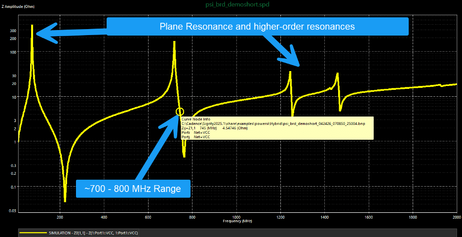
Figure 2: PDN impedance vs frequency showing multiple cavity resonances. These peaks are driven by plane dimensions, dielectric spacing, and via distribution. Not regulator performance.
Parallel plane pairs do not just store charge. They behave as cavity resonators. The plane edges reflect electromagnetic energy back toward the center. At specific frequencies, the reflections add in phase and the cavity rings.
The first resonance frequency is approximately the speed of light divided by twice the longest plane dimension times the square root of the dielectric constant. For a 4-inch plane dimension with a dielectric constant near 4, the first resonance falls near 740 MHz. At that frequency, the plane impedance spikes. Any via that penetrates the plane pair at a resonance hotspot couples that noise into whatever signal uses the via.
Complex high-speed PCBs often have several power rails with large plane areas. Each one has its own set of resonance frequencies set by its shape. At this stage of the PCB design, power integrity is no longer just a component-level concern, it becomes a system-level interaction between geometry and frequency behavior.
Sigrity X Aurora can compute those resonances and show you a heat map of where they peak on the board. The following results are generated from a representative demonstration layout to illustrate how plane geometry shapes PDN behavior. Those hotspots are where you do not want to place sensitive analog lines or high-speed serializers.
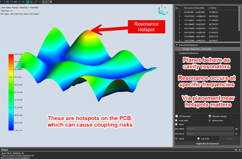
Figure 3 : Resonance mode of a power-ground plane pair at a specific frequency. The spatial distribution reveals geometry-driven hotspots where noise coupling is strongest.
Those hotspots are where you do not want to place sensitive analog lines or high-speed serializers.
Stitching Vias Break the Cavity
A stitching via ties a power plane to its ground plane reference. Each stitching via locally reduces the impedance between the power and ground structures, altering the cavity current distribution and suppressing resonant behavior. Many stitching vias, distributed across the plane area, suppress cavity resonances by lowering the Q factor of the structure and reducing the size of uninterrupted resonant regions .
This is geometry, not component selection. You do not buy low-resonance vias. You place more of them and put them in the right locations. The locations that matter most are near every signal via that transitions between layers. When a signal via penetrates the power and ground planes, the electromagnetic wave has to make the same transition. The nearest stitching via is where that wave’s other half couples to its nearest lowest impedance conductor and voltage reference.
If the nearest stitching via is far away, the electromagnetic waves traverse any and all PCB surfaces and dielectric material it needs to, to find its reference voltage. All conductive materials in that path have their electrons excited, thus forming an incident current path in the process. A large path has more inductance. More inductance means more voltage drop at the return transition. That voltage drop is the noise on your PDN.
Putting It Together on any Complex High-Speed Board
On a typical multi-layer PCB, the highest-current rails span large plane areas. Without sufficient stitching, these planes can resonate in the hundreds of megahertz range, well within the spectral content of modern switching loads.
Run PDN impedance analysis on the layout database. Look at the impedance as a function of frequency. Look for peaks. Peaks are resonance. The goal is to keep PDN impedance below the target impedance across the operating frequency range of the load. When impedance exceeds the target, transient current demand converts directly into voltage ripple on the power rail. Correlate the peak frequencies to plane dimensions. Then place stitching vias to break up the largest cavities.
The visual payoff is immediate. Before: impedance peaks near the resonance frequencies. After: the peaks flatten. The PDN maintains lower impedance and reduced voltage ripple across the frequency band your signals care about, improving overall power distribution
The Geometric Controls in Order
Power integrity comes from three geometric choices, in this order of influence:
First, the PCB stackup. Closer plane pairs, thinner dielectric, more distributed capacitance. The Cross-Section Editor sets this once and it affects the whole board, making it one of the most critical steps in the design process.
Second, the plane shape. Long, narrow planes resonate at lower frequencies than short, compact planes. Cutouts and voids change the cavity dimensions in ways that can surprise you. Look at your planes the way an antenna designer looks at a patch.
Third, the stitching via pattern. Enough stitching vias, placed where signal transitions happen, break up the cavities and complete the electromagnetic field wave guidance and subsequently the induced current paths.
Change the geometry, and you change the power delivery. The schematic defines the voltage target, but it is the copper that ultimately determines what the IC receives.