Why Rule-Based Signal Integrity Checks Miss EMC Issues
Your design passes design rule check ( DRC ) with zero violations. Every trace meets the spacing rule. Every differential pair is length-matched within tolerance. The board ships to fabrication, returns from fabrication and fails signal integrity (SI) validation at 8 Gbps. What did the DRC checks miss?
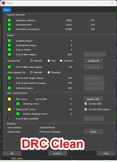
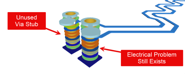
Figure 1: A board can pass DRC and still fail electrically. Here, the geometry is legal, but the through-hole via leaves an unused stub that can create a high-frequency discontinuity
What Rules Actually Check
Design rules check geometry, trace width, clearance between traces, length matching across a bus, via count on a net, and drill hit spacing on a panel.
These are useful checks. They catch manufacturing problems early and enforce the tolerances your fabricator needs to build the board.
However, they are not enough. A spacing rule of 5 mils does not tell you whether crosstalk at 10 GHz exceeds your noise budget in high speed designs. A length-matching rule of plus or minus 50 mils does not tell you whether the resulting skew, reflections, and interconnect loss reduce timing margin enough to close the eye diagram at the receiver . The rules answer one question: is the geometry within tolerance? They cannot answer the more important question: will the signal arrive clean?
The limitation is that DRC systems evaluate static geometry against predefined constraints, while signal integrity and EMC problems are fundamentally frequency dependent electromagnetic behaviors. Whether a structure causes reflections, coupling, or radiation depends not only on its dimensions, but also on edge rate, dielectric properties, reference plane behavior, and the spectral content of the signal moving through it.
Three Failure Modes That Pass DRC
Geometric rules are not able to account for electrical engineering context. This means you can still get critical signal integrity problems that slip through the cracks if you’re not actively analyzing the electric field behavior. In fact, there are three primary ways a board can consistently pass a DRC but still lead to hardware failure.
1. Via stub resonance. A through-hole via with an unused stub can pass every standard DRC while still creating a high-frequency discontinuity. In FR-4 with a dielectric constant near 4, a 60-mil stub produces resonance behavior in the multi-gigahertz range, with the quarter-wave resonance occurring near 24 GHz. The resonance relationship is straightforward: frequency equals the speed of light divided by four times the stub length multiplied by the square root of the dielectric constant. Even before full quarter-wave resonance occurs, the via stub introduces frequency-dependent reflections and insertion loss degradation that reduce channel margin. A 10 Gbps serial link may see this as a notch in insertion loss or increased reflection energy at higher harmonics. In many high-speed systems, the signal edge rate is often more important than the nominal bit rate when evaluating discontinuities. Fast rise times contain energy far into the multi-gigahertz range, allowing via stubs, plane resonances, and impedance discontinuities to affect the signal even when the fundamental data rate appears relatively low. The DRC does not detect the problem because the failure depends on stub length, dielectric constant, rise time, and signal spectrum together. Geometry alone does not predict the electrical behavior.
2. Return path discontinuity. A signal routed across a plane split passes spacing and width checks. The DRC does not check whether the return current has a continuous path beneath the trace. High-frequency return current flows on the reference plane directly under the signal. At high frequencies, return current follows the path of lowest impedance. Because electromagnetic fields are tightly coupled between the signal trace and its reference plane, the return current naturally concentrates directly beneath the routed trace as a byproduct of the electromagnetic field. When the reference plane is interrupted by a split or void, the electromagnetic fields spread outward to find the nearest low-impedance reference conductor, creating multiple electron movement (current) effects, increasing loop area and inductance as a result. If that plane has a gap, the field induces return current that detours around the gap. The detour increases loop inductance. As the field and waves spread around the discontinuity, part of the differential signal energy can induce common-mode current into the surrounding copper from the superimposed waves. Common-mode currents are especially problematic because they radiate efficiently from board edges, attached cables, connector structures, and plane cavities. This is why a layout that passes geometric spacing and width rules can still fail EMC testing due to excessive radiated emissions. The signal picks up common-mode noise. Emissions go up. And none of this shows in the DRC report for routed traces.
3. Crosstalk accumulation. Two traces with 5-mil (0.127 mm) spacing and running in parallel with each other for 200 mils (5.08 mm) will each pass the spacing rule individually. When multiple aggressors propagate signals that are switching (changing voltage) simultaneously on the same layer, the cumulative coupling can eat up the noise margin on the victim nets. The DRC checks each pair in isolation. It does not sum the coupling from multiple aggressors. The failure appears as jitter or data errors during lab testing, long after the fabrication clock starts.
What Electrical Analysis Catches
Sigrity X Aurora reads the routed Allegro X PCB Layout database directly. You do not need to export to another tool or rebuild the geometry. You run the analysis on the actual copper.
For via stubs, the Impedance workflow shows impedance as a function of distance along the signal. Each via transition appears as a dip or spike. You see the severity of each discontinuity or impedance mismatch before the board is built.
For return paths, the reference plane analysis shows whether the plane beneath each signal segment is continuous. Gaps, splits, and void regions show up as colored overlays on the layout canvas. You can jump from the report directly to the problem location within the canvas in Allegro X PCB Layout and fix it.
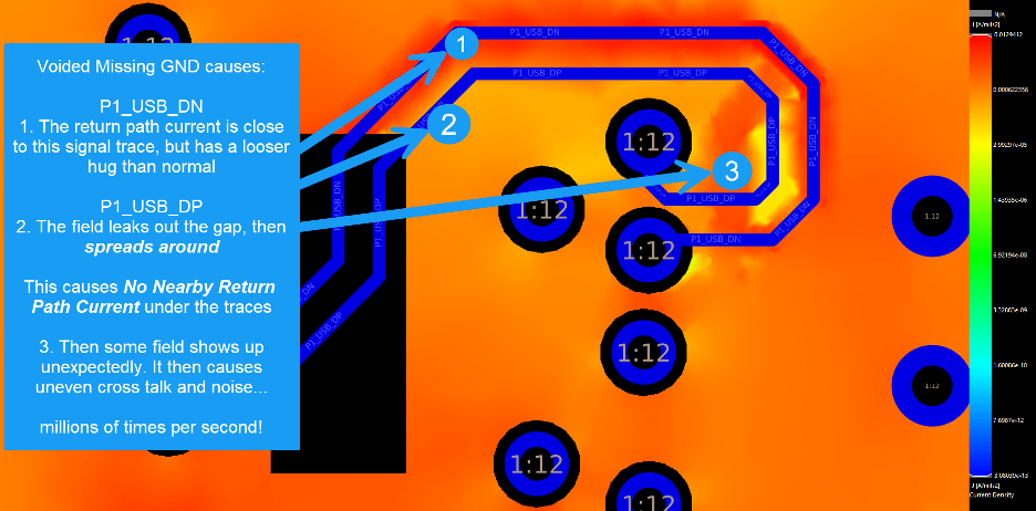
Figure 2 : Return path problems often pass standard rule checks. The signal trace may be legal, but a gap in the reference plane forces return current to detour, increasing loop inductance and emissions.
For crosstalk, the Impedance and Coupling workflow identifies which nets couple to which. The Crosstalk and Reflection workflow then calculates near-end crosstalk (NEXT) and far-end crosstalk (FEXT) for those pairs. You get actual voltage numbers tied to actual geometry. You see whether the crosstalk budget holds up with all aggressors active.
Why This Matters for Your PCB Design Schedule
Every re-spin costs two to four weeks for fabrication and assembly, along with engineering time to diagnose the failure and the cost of the scrapped boards. The analysis that would have caught the failure takes an afternoon during routing.
The tradeoff is not complicated. You can run the checks early, while the fix is a routing change, or you can run them late, when the fix is a new revision.
Design rules enforce what the fabricator needs to build your board. Electrical analysis enforces what the signal needs to arrive clean. You need both.