Electromagnetic Side Effects of HDI: Cavity Modes, Return-Path Fragmentation, and Plane Resonance Patterns
HDI technology delivers remarkable routing density gains, but the electromagnetic behavior of dense microvia fields differs fundamentally from conventional through-hole designs. As signal frequencies climb into multi-gigahertz ranges, the interaction between microvia structures and reference planes creates resonance phenomena that can compromise signal integrity and generate EMI problems invisible to traditional analysis methods.
Understanding these electromagnetic side effects is essential for designing HDI boards that perform cleanly at high frequencies.
How Microvia Fields Create Cavity Modes
A pair of parallel reference planes separated by dielectric material forms a parallel-plate waveguide, a structure capable of supporting resonant electromagnetic modes. In conventional PCBs, the relatively sparse distribution of through-hole vias provides sufficient plane-to-plane shorting to suppress these resonances below frequencies of practical concern.
HDI designs change this equation. Microvia fields are denser than through-hole patterns, but microvias only connect adjacent layer pairs. Unlike through-vias that short all planes they penetrate, a microvia connecting layers 1-2 provides no damping for resonances between layers 3-4, 5-6, or other plane pairs in the stackup.
The result is that HDI stackups can exhibit plane resonances at lower frequencies than equivalent-layer-count through-hole designs. These resonances create frequency-dependent impedance variations in the power delivery network and can couple noise into signal vias that penetrate the resonant cavity.
The resonant frequencies depend on plane geometry and dielectric properties. For a rectangular plane pair, the fundamental resonance occurs when the plane dimension equals half a wavelength in the dielectric medium. A 4-inch plane dimension with Er=4 resonates around 740 MHz, which is well within the spectral content of modern high-speed signals.
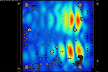
Figure 1: Identifying "No-Fly Zones" for sensitive signals. Full-wave EM analysis reveals high-impedance resonance peaks. Placing sensitive analog lines or high-speed serializers in the red "hotspots" can compromise signal integrity due to ground bounce and coupling
Preventing Return-Path Discontinuities
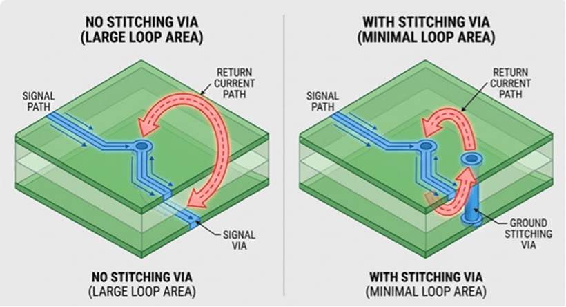
Figure 2: The Loop Area Problem. The left diagram shows the large inductive loop created when the current return must wander to find a path between layers. The right diagram shows how a stitching via provides an immediate bridge, minimizing the loop area and reducing radiated emissions.
Return current follows the path of lowest impedance, which at high frequencies, effectively means the path of lowest inductance, directly beneath the signal trace on the nearest reference plane. When a signal transitions between layers, its return current must also transition between reference planes. Without a low-impedance path for this transition, return current is forced to find alternative routes, creating loops that radiate and increasing the effective inductance of the signal path.
In through-hole designs, signal vias and their associated ground vias typically penetrate all layers, providing automatic return-path continuity. HDI complicates this: a signal microvia from layer 1 to layer 2 may reference a ground plane on layer 2, but if that signal continues deeper into the board via another microvia from layer 2 to layer 3, the return current needs a path from the layer-2 ground to whatever reference exists on layer 3.
Effective return-path management in HDI requires explicit stitching strategies:
- Ground stitching vias: Place ground microvias adjacent to signal microvias at every layer transition. The closer the stitching via to the signal via, the smaller the return-current loop and the lower the transition inductance.
- Reference plane continuity: Design stackups so that signal layer transitions occur between layers that share a common reference plane, or ensure explicit stitching connects the relevant references.
- Via pattern planning: Under dense BGAs where signal vias are tightly packed, ensure the via pattern includes adequate ground vias distributed throughout the field, not just at the periphery.
Strategies to Stop Plane Resonance Hotspots
Plane resonances create spatial patterns of high and low impedance across the board surface. Signals or power connections located at impedance peaks experience maximum noise coupling; those at nulls see minimal effect. Unfortunately, component placement is driven by functional requirements, not resonance avoidance, so some critical signals inevitably land at problematic locations.
Several strategies mitigate plane resonance effects in HDI designs:
Distributed stitching via arrays: Use via arrays to connect plane pairs throughout the board and not just at edges of the PCB. Using them everywhere you have space distributes how you handle your shorting of signals between same net planes, raises resonant frequencies and reduces Q-factor. In HDI, this requires planning stitching via locations that don't conflict with routing channels, using via types appropriate to each plane pair.
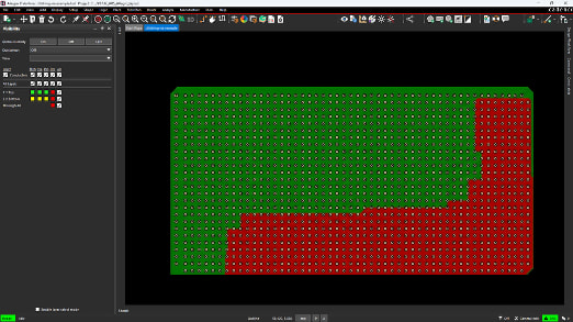
Figure 3: Distributed stitching via array implemented in Cadence Allegro X. Exaggerated approach
A distributed via array acts as a "shorting grid" to suppress plane resonance hotspots before they can form. While the above image is an exaggerated example (one may use fewer vias), this is not uncommon when you have multiple return paths or zero reference layers adjacent to one another.
Embedded capacitance: Thin dielectric layers between power and ground planes increase distributed capacitance, which lowers the characteristic impedance of the plane pair and shifts resonances. HDI stackups with 2-3 mil dielectrics inherently provide more distributed capacitance than conventional designs.
Split plane management: Where multiple power domains require split planes, the splits create edge discontinuities that reflect energy and can generate their own resonance modes. In HDI designs, route signals that cross splits on layers with continuous reference planes, and stitch across splits with capacitors where DC isolation is required.
Lossy materials: Higher-loss dielectric materials damp resonances more effectively. While low-loss materials are desirable for signal integrity, using standard-loss materials for plane-pair dielectrics can reduce resonance amplitude without significantly affecting signal path performance.
EM Modeling Insights for Dense HDI Areas
Traditional signal integrity simulations using transmission-line models or 2D field solvers may not capture the full electromagnetic behavior of dense HDI regions. The interaction between closely-spaced microvia fields, thin dielectric layers, and reference plane geometry creates three-dimensional field distributions that require full-wave EM analysis to characterize accurately.
Key areas where EM modeling provides essential insight include:
- Via-to-via coupling: In dense microvia fields, electromagnetic coupling between adjacent vias can create crosstalk paths that don't appear in schematic-level analysis. EM extraction quantifies these coupling mechanisms.
- PDN impedance: The impedance of power delivery networks through microvia fields differs from simple via inductance models. The distributed nature of microvia connections and their interaction with plane resonances requires EM simulation to characterize accurately.
- BGA breakout regions: The area directly beneath fine-pitch BGAs concentrates signal, power, and ground vias in a small region. EM simulation of this region reveals coupling paths and return-current distributions that inform via placement and stitching strategies.
- Cavity resonance identification: EM eigenmode analysis identifies resonant frequencies and mode shapes for plane pairs, highlighting regions of high field concentration where sensitive signals should be avoided.
Tools like Sigrity X PowerSI and Clarity 3D Solver provide the extraction and analysis capabilities needed to characterize these effects. Investing in EM analysis for critical HDI regions early in the design process avoids costly surprises during validation.