What I’ve Learned About Impedance, Decoupling, and Planes That Changed My Approach
If you've ever had a design that worked flawlessly in simulation but failed spectacularly on the bench, you're in good company. I remember one of my early projects, a high-speed digital board with a sleek stack-up and textbook signal routing. Everything looked perfect on paper. But once we powered it up, I saw voltage ripple that danced all over the scope and logic that glitched under load. That was my wake-up call to the world of power integrity.
Power integrity, or PI, isn't a buzzword or a nice-to-have. It's a foundational part of PCB design that determines whether your components receive the power they need, at the right voltage and with minimal noise, across all operating conditions. Over the years, I've come to think of PI as a three-legged stool held up by impedance control, capacitor strategy, and smart use of power and ground planes. In this post, I'll share the core lessons that reshaped how I design circuit boards.
Understanding Power Integrity and Why It's Not Optional

Power integrity is all about ensuring that every IC, whether it's a microcontroller or a power-hungry FPGA, receives a stable and clean power supply throughout its operational frequency range. It's easy to focus on signal integrity and forget that power delivery can undermine everything. Poor PI leads to voltage dips, ground bounce, increased EMI, and system instability.
In modern high-speed designs, power is no longer just about supplying DC voltage. It's about handling high-frequency transient currents that can spike and drop in nanoseconds. The traditional view of power as a static supply rail doesn't hold up. Instead, I now design power delivery networks (PDNs) as dynamic systems that respond to frequency and load variation.
If your design includes DDR memory, high-speed transceivers, or processors with aggressive switching, power integrity must be considered from the beginning. This starts with understanding impedance.
Impedance and the Myth of 'Low Resistance'
It took me a while to unlearn the idea that low resistance equals good power delivery. In truth, it's impedance, not just DC resistance, that matters. Impedance is frequency-dependent. At DC, your power trace or plane might look fine. But at 100 MHz or 1 GHz, inductive effects dominate, and impedance can skyrocket.
There's a concept called target impedance (Ztarget), defined as:
Ztarget = Vripple / Itransient
Based on the acceptable ripple and expected transient current, this gives you the maximum allowable impedance your PDN can have over a certain frequency range. If your PDN exceeds this, your voltage will dip or spike, possibly outside the operating tolerance of your ICs.
Voltage regulators (VRMs) have limited bandwidth and can't respond fast enough to high-frequency events. That means the board-your traces, planes, and decoupling capacitors-must handle those fast transient currents. The goal is to keep the impedance flat and below Ztarget from low MHz into the GHz range.
Capacitors: More Than Just Bulk and Bypass

If impedance is the "what," then capacitors are a big part of the "how." I used to sprinkle 0.1uF capacitors everywhere, assuming more was better. But without understanding ESL (equivalent series inductance) and ESR (equivalent series resistance), it's easy to waste board space and still miss your PI targets.
You need capacitors that cover a wide frequency spectrum:
- Bulk capacitors (10-100μF) for low-frequency stability
- Mid-frequency caps (1-10μF) to bridge the gap
- High-frequency caps (0.01-0.1μF) close to ICs for fast response
But stacking ten identical 0.1uF caps won't help much if their ESL is too high. Instead, I use a parallel mix of capacitor values to create a wide-band response. Placement is also critical: put high-frequency caps as close to power pins as possible, and minimize the loop area between cap and IC.
Another trick is placing capacitors directly under BGAs on inner layers, with via-in-pad and reverse geometry packages, to reduce inductance. The lower the ESL, the better the cap performs at high frequencies.
Planes: The Unsung Heroes of Power Delivery
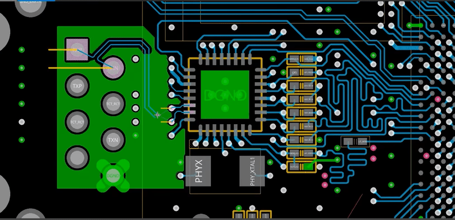
The third leg of the PI stool is your power and ground planes. These planes aren't just copper fills; they're transmission structures that carry return currents and form distributed capacitance.
A solid ground plane is your best friend. It lowers loop inductance, provides a return path for high-speed signals, and forms the base for stable power delivery. Avoid ground splits unless absolutely necessary. In my designs, I make sure every signal crossing a boundary has a nearby return via to avoid disrupting return current flow.
When designing stack-ups, I favor configurations where power and ground planes are adjacent, ideally separated by a thin dielectric to create embedded capacitance. This plane capacitance can offer low-inductance decoupling right where it's needed.
Avoiding power plane cutouts, using via fences around high-speed regions, and stitching caps across plane transitions all help maintain a low-impedance path. One of my favorite hacks is using a via array under dense ICs to form a low-inductance connection between planes.
Lessons Learned: What I Do Differently Now
I used to treat power delivery as an afterthought. Now, I start every high-speed board layout with a PDN strategy session. I simulate impedance profiles using tools like PIPro or Sigrity, and I optimize stack-ups for power first, not just routing space.
In one project, adding a dedicated ground layer and switching from split power planes to a contiguous PDN dropped the ripple from 120mV to under 20mV. The system passed EMI testing on the first try, a rare and satisfying result.
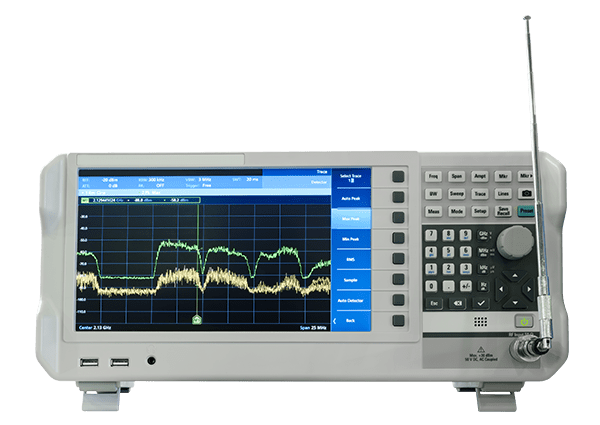
I also learned to model capacitors in simulation, not just assume their datasheet performance holds at high frequencies. Real-world testing with a VNA (vector network analyzer) showed me just how different the board behaves from the theory.
Conclusion: Your Power Integrity Checklist
If I had to boil down years of PI struggles into a few rules, here's what I would tell any fellow engineer:
- Know your Ztarget and simulate your PDN across the frequency range.
- Use capacitors intentionally, with varied values and tight placement.
- Design your planes to support power, not just route it. Keep them solid, adjacent, and uninterrupted.
- Avoid shortcuts like ground pours without return planning or blindly trusting layout defaults.
- Measure when possible - what you don't measure can (and will) fail you.
Power integrity is an invisible force that makes your design hum or sends you chasing ghosts in the lab. Don't wait for the oscilloscope to show you what your layout missed. Design for power integrity from the start, and your future self will thank you.
If you're working on your next PCB, I challenge you to look at your PDN like a system, and not as an afterthought. Power integrity isn't glamorous, but it separates good designs from great ones.