PCB Stackup Planner
Key Takeaways
-
PCB stackup planning dictates electrical performance, manufacturability, and reliability, ultimately leading to successful PCB design.
-
Optimizing stackup involves careful consideration of layer arrangement, material selection, and impedance control.
-
OrCAD X features built-in impedance calculators, simulation tools, and more that can assist in PCB stackup planning.
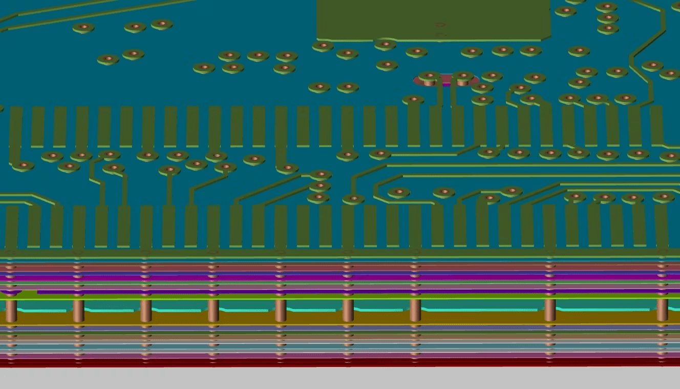
3D view of a multi-layered PCB Design
Designing a PCB can feel a bit like building a house. When building a house, you wouldn't start hammering nails without a blueprint? Similarly, before routing a single trace, a well-defined PCB stackup is essential. It's the foundation upon which your entire design rests.
So, what exactly is a PCB stackup planner? Simply put, it's the design tools or functions that help you choose and arrange the copper and insulating layers of the PCB stackup. The stackup dictates the electrical performance, manufacturability, and, ultimately, the reliability of your final product. Getting it right from the start can save you headaches down the road. Let’s look at overall considerations for a PCB stackup planner.
PCB Stackup Planner: Overall Considerations
|
Consideration |
Description |
|
The number of layers directly influences routing density and signal integrity. More layers allow for more complex routing and dedicated ground/power planes but also increase cost and board thickness. |
|
|
Layer Arrangement |
Signal layers should be adjacent to ground planes to provide a low-impedance return path and minimize crosstalk. Power planes should be closely coupled to ground planes to provide decoupling capacitance. |
|
Material Selection |
The choice of dielectric materials (e.g., FR-4, Rogers, etc.) affects the dielectric constant (Dk) and loss tangent (Df), which, in turn, influences signal propagation speed and signal loss. High-speed designs often require materials with low Df. |
|
Copper Weight |
The thickness of the copper layers (specified in ounces per square foot) affects the current-carrying capacity and impedance of traces. Higher copper weights are needed for power planes and high-current signals. |
|
The thickness of the dielectric layers affects the impedance of traces and the capacitance between layers. It also influences the overall board thickness and flexibility. |
|
|
Impedance Control |
Controlling trace impedance is achieved by carefully selecting the trace width, dielectric thickness, and copper weight. Controlled impedance is essential for high-speed signals to prevent reflections and signal degradation. |
|
Via Types |
The type of vias used (e.g., through-hole, blind, buried) can also affect signal integrity and routing density. Blind and buried vias allow for more efficient routing but also increase manufacturing costs. |
PCB Stackup Planner: Approaching The Process
To illustrate how these considerations come into play during the PCB stackup planner process, let's briefly walk through the early stages of a typical design scenario. Let's say you're designing a mixed-signal board that includes both high-speed digital circuits and sensitive analog circuits. Here's how the stackup process would start:
-
Identify Critical Signals: Determine which signals require controlled impedance and which are particularly sensitive to noise.
-
Define Ground Planes: Dedicate one or more layers to ground planes. These planes provide a low-impedance return path for signals and shield sensitive circuits from noise.
-
Isolate Analog and Digital Sections: Physically separate the analog and digital sections of the board to minimize noise coupling. This might involve using separate ground planes for each section.
-
Determine Layer Count: Based on the routing density and signal integrity requirements, determine the number of signal layers needed.
-
Select Materials: Choose appropriate materials for the core and prepreg layers. Consider factors such as dielectric constant, loss tangent, and cost.
-
Create a Stackup Diagram: Draw a diagram that shows the arrangement of all the layers, including the copper weights and dielectric thicknesses.
The Key Aspects of Stackup Planning
Layer Arrangement
If your PCB stackup were now a sandwich, we realize just how impactful the order of the layers becomes. Signal layers should be adjacent to ground planes. This provides a low-impedance return path, which minimizes signal reflections and crosstalk. Crosstalk, by the way, is when a signal on one trace bleeds over and interferes with a signal on another trace.
Power planes should also be closely coupled to ground planes. This creates decoupling capacitance, which helps to suppress noise on the power rails. Noise on the power rails can wreak havoc on sensitive analog circuits.
Material Selection
The materials you choose for your PCB stackup play a large role in its performance. The two key properties to consider are the dielectric constant (Dk) and the loss tangent (Df).
-
Dielectric Constant (Dk): This is a measure of how much electric field energy can be stored in the material. A lower Dk generally results in faster signal propagation speeds.
-
Loss Tangent (Df): This is a measure of how much signal energy is lost as it propagates through the material. A lower Df results in less signal loss.
For high-speed designs, you typically want materials with low Dk and low Df. Common materials include FR-4, which is a standard, cost-effective option, and Rogers materials, which offer superior performance but come at a higher price.
Impedance Control
Controlled impedance refers to managing the characteristic impedance of a PCB transmission line formed by traces and their associated reference planes. This is essential for maintaining signal integrity at high frequencies by preventing signal distortion. It is determined by the physical dimensions and dielectric materials of the PCB and is measured in ohms (Ω).
Common PCB transmission lines requiring controlled impedance include single-ended microstrip, single-ended stripline, microstrip differential pair, stripline differential pair, embedded microstrip, and coplanar lines (both single-ended and differential). Achieving controlled impedance involves matching substrate material properties with trace dimensions to ensure the impedance remains constant along the entire PCB path—from source to destination—regardless of trace routing or layer changes.
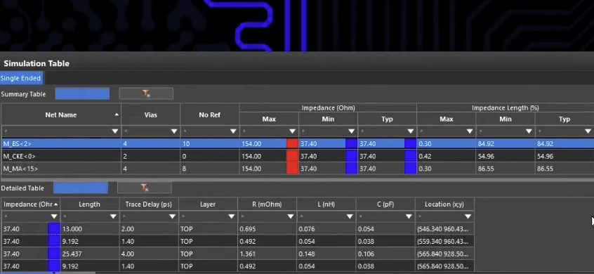
Easily find which traces in your design that have the highest impedance
OrCAD X and the PCB Stackup Planning Process
OrCAD X offers a suite of tools that can streamline the stackup design process and ensure signal integrity:
-
Impedance Control Calculator: OrCAD X has built-in impedance calculators that allow you to calculate the impedance of traces based on their dimensions and material properties. You can specify your target single-ended or differential impedance values, and OrCAD X will automatically recalculate the necessary trace widths and spacing. For instance, setting a target single-ended impedance of 50 Ω will prompt OrCAD X to adjust the trace width accordingly, accounting for variations between outer and inner layers due to differing dielectric materials.
-
Simulation Tools: OrCAD X has simulation tools that allow you to simulate the performance of your stackup before you even build a prototype. OrCAD X also allows you to extract and model any net or differential pair into the Topology Explorer for advanced simulation and to enforce ideal interconnect constraints.
-
DFM Checks: OrCAD X includes Design for Manufacturability (DFM) checks that can help you identify potential manufacturing problems with your stackup. This can save you time and money by preventing costly manufacturing errors.
-
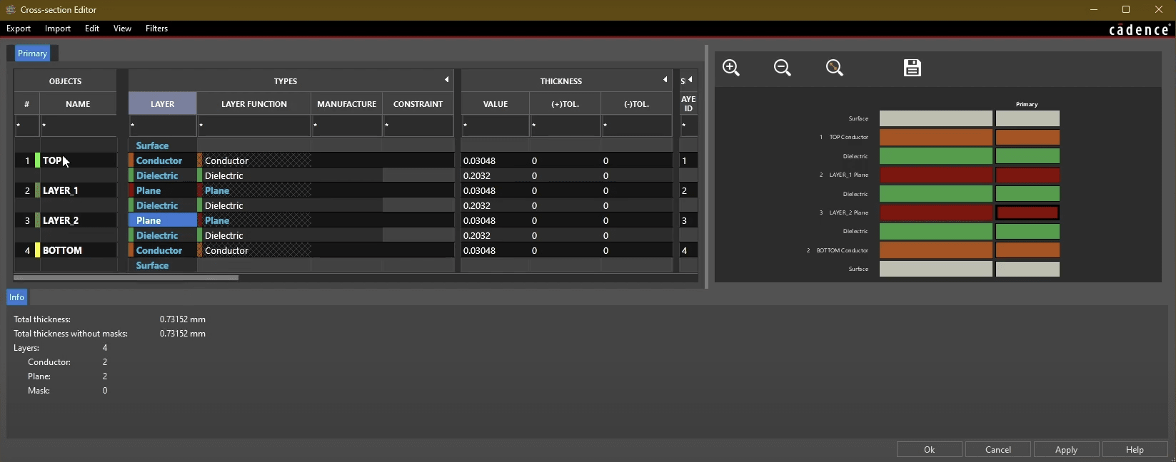
Cross-Section Editor: The cross-section editor in OrCAD X allows you to visualize your stackup in a graphical format. You can define the layer arrangement, material properties, and copper weights. This provides a clear picture of your stackup and helps you identify potential problems.
Don't leave building your PCB house to chance, and make sure your PCB stackup planner is the best it can be. OrCAD X provides the comprehensive tools you need to design, simulate, and collaborate on your stackup, ensuring optimal performance and manufacturability. Ready to take control of your PCB design process? Get started with an OrCAD X Free Trial today.
Leading electronics providers rely on Cadence products to optimize power, space, and energy needs for a wide variety of market applications. To learn more about our innovative solutions, subscribe to our newsletter or our YouTube channel.