Grounding and Return Paths: Advanced Techniques - Part Two
Component Placement to Minimize Return Path Length
Component placement plays a vital role in minimizing return path length in high-speed PCB designs. As current flows through components, it must find its way back to the source - a simple yet significant concept that helps maintain signal integrity.
Critical Component Positioning for Clean Return Paths
Organizing components effectively, particularly through functional grouping, is essential for establishing clear and efficient return paths. High-speed sections need critical components positioned based on these factors:
- Place parts of related signal paths in close proximity to minimize the current loop area
- Position receivers as close as possible to signal inputs to reduce delays
- Avoid placing components that aren't part of a circuit between components of that circuit
- Organize functional blocks (power, RF, digital, analog) as groups to minimize signal crossing
- Keep sensitive high-speed devices away from board edges to reduce EMI
Complex designs often have component pin density exceeding 110 pins per square inch, making careful positioning essential. The receiver part should sit as close as possible to the input. Such an arrangement creates the smallest loop area and significantly reduces signal path delays. Reference ground points stay "quiet" without undesirable current flow interference.
Signals traveling over power planes share electric fields with those planes, allowing noise to propagate into signal lines. Components need to be placed so high-speed signals don't cross splits in power planes, which breaks return paths. Parts should maintain continuous return paths on reference planes.
Decoupling Capacitor Placement for Ground Bounce Prevention
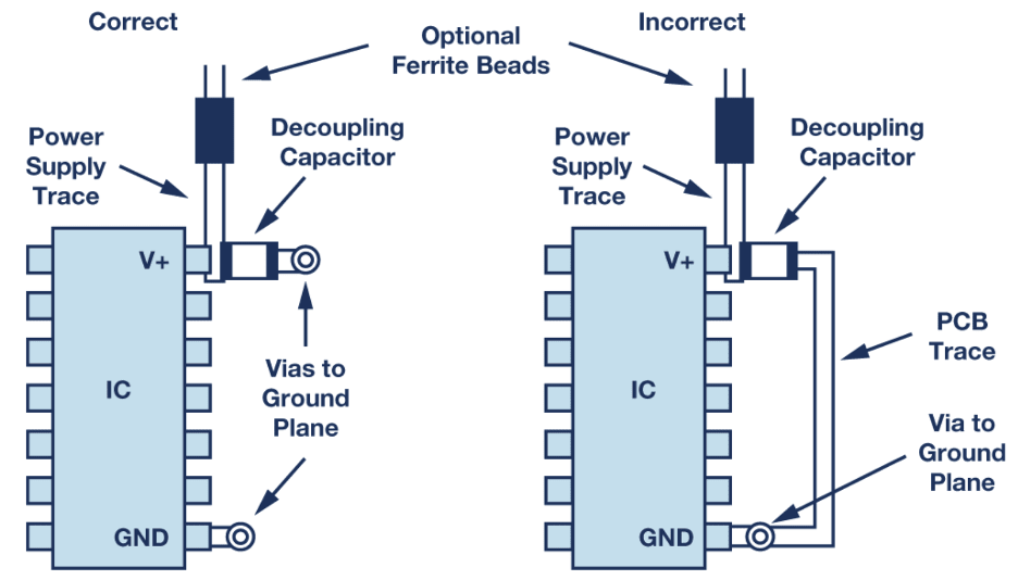
Image Credit: Analog Devices - Grounding and Decoupling
Ground bounce occurs when voltage fluctuations arise between an IC's output and the PCB ground plane during switching. To mitigate this issue, strategic placement of decoupling capacitors is essential.
The bypass capacitors should sit as close as possible to IC power input pins. Increased distance creates excessive inductance that can cause resonance effects and higher impedance. Here's how you can prevent or minimize ground bounce effectively:
- Position bypass/decoupling capacitors directly at IC power supply pins
- Place the lowest-value capacitor closest to the device pin
- Connect capacitors directly to power/ground planes using multiple vias
- Space limitations might require capacitors on the opposite side of the board underneath ICs
Using multiple parallel capacitors of different values is an effective way to maintain low AC impedance across a wide frequency band, ensuring that power supply pins are stable. This approach minimizes impedance for power compensation and reduces voltage droop during capacitor charge/discharge cycles.
Regardless of design complexity, using two local decoupling capacitors works better than one with double the value. By placing capacitors in parallel, the equivalent series inductance (ESL) and resistance (ESR) are reduced, improving performance in high-speed circuits.
Routing Techniques That Preserve Return Path Integrity
Signal quality in high-speed designs depends on the integrity of the return current path. The way current seeks the path of least impedance creates the foundation for effective routing strategies.
Maintaining Continuous Return Paths Under Traces
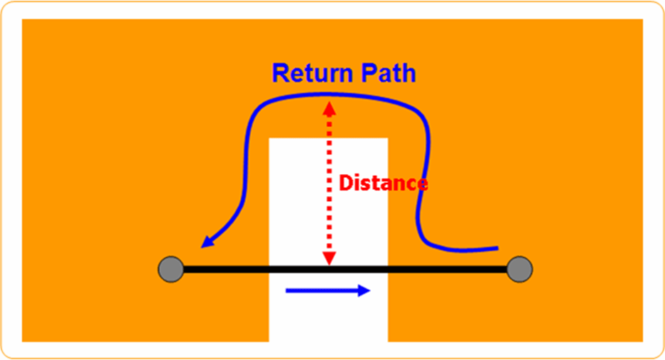
Image Credit: Altair - Return Path
High-frequency return currents flow directly beneath signal traces instead of spreading through the ground plane. Return current concentrates tightly underneath traces at frequencies above 10 MHz, creating a specific distribution pattern. Designers should avoid discontinuities like voids, slots, or clearance holes in reference planes. These force current to take detours, which creates larger loop areas and increases inductance.
Crossing Split Planes Safely with Stitching Capacitors
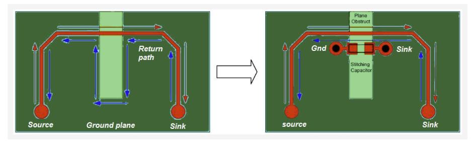 Image Credit: Sierra Circuits - Proto Express ® - 11 Best High-Speed PCB Routing Practices
Split planes create return path discontinuities that significantly affect signal integrity. Stitching capacitors are crucial when traces must cross splits. These capacitors act as bridges between reference planes and provide paths for high-frequency return currents. Research shows that well-implemented stitching capacitors reduce crosstalk by up to 10 dB. The best results come from:
- Capacitor placement directly at trace crossing points
- Values between 0.1µF and 10nF
- Multiple capacitors for critical signals
- Low ESR and ESL to minimize impedance
Differential Pair Routing for Improved Return Path Control
Differential pairs are great for return path management. They minimize electromagnetic interference through field cancellation and provide immunity to common-mode noise. Here are some successful differential routing principles to follow:
- Consistent trace width and spacing throughout
- Equal trace lengths (within tolerances like 150 mils for USB, 25 mils for DDR2)
- Pairs staying together while allowing separation around obstacles when needed
- Return path vias positioned near signal vias during layer transitions
Managing High-Speed Bus Routing and Termination
Maintaining consistent impedance throughout the length of high-speed busses is crucial to ensure proper signal integrity. To avoid impedance discontinuities, designers should minimize the use of vias even at lower data rates. When busses transition across multiple layers, ground vias should sit symmetrically near signal vias toThis maintain continuous return paths. Additionally, proper transmission line termination is essential to prevent reflections. And depending on an interface's requirements, designers can use series termination at the driver or parallel termination at the receiver.
Practical Grounding Solutions for Common Interfaces
High-speed interfaces have unique grounding challenges, each requiring specific solutions. Implementing proper grounding techniques help maintain signal integrity and reduce EMI concerns.
DDR4/DDR5 Memory Grounding Requirements
Modern memory interfaces naturally include multiple grounded lines. DDR4/DDR5 specs feature pin layouts with multiple ground connections. This creates dedicated return paths for each signal in the interface. The architecture minimizes loop areas and effectively controls impedance.
DDR5 designs run at speeds above 5200 MT/sec/pin. This means they need stricter grounding than previous versions. DDR5 uses decision feedback equalization (DFE) to handle channel losses and dispersion in DQ lines. This works well when reflection losses dominate channel behavior. A consistent ground reference becomes essential.
Your DDR will work best if you:
- Keep ground planes continuous under memory traces
- Route memory signals away from split planes
- Add ground vias next to signal vias during layer transitions
- Follow the memory controller's termination requirements
USB 3.x and PCIe Return Path Management
PCIe and USB 3.x interfaces run at 5-Gb/s and require careful return path management. Both use high-speed differential signaling and return path quality directly affects their performance.
These interfaces work best when transmit (TX) and receive (RX) pairs stay separate. The TX and RX differential pairs should ideally be five times the trace width apart (5W rule). If space is tight, maximize the gap between pairs and add ground-fill. Another option is to route each differential pair on opposite board sides with a ground plane between them.
Key points to remember:
- Stub lengths should stay under 15 mils for vias in high-speed traces above 5Gbps
- Ground vias should surround signal vias to keep the return current close
- Signals should avoid gaps in reference planes
- Split ground planes need one connection point to prevent ground loops
RF and Microwave Circuit Grounding Techniques
RF and microwave circuits face unique grounding challenges. At high frequencies, even minor physical structures add parasitic impedances, leading to issues such as parasitic inductance, ground loops, and EMI coupling.
Parasitic inductance in ground connections creates voltage differences between ground points, making it hard to maintain consistent references across amplifiers. These effects change impedance matching, raise insertion loss, and lower power efficiency.
RF/microwave grounding works best when you:
- Use continuous ground planes without many cuts or slots
- Shield circuits from EMI properly
- Keep high-power and low-power components ground-isolated
- Connect all grounds to common points, often called "star grounding"
- Use separate analog and digital power supplies with their respective grounds for mixed-signal designs
Grounding Fundamentals Summarized
Proper grounding is the lifeblood of successful high-speed PCB design. Our exploration of grounding principles shows how return paths affect signal integrity, EMI performance, and overall circuit reliability.
Ground-related problems demonstrate themselves in many ways - from signal degradation and EMC test failures to mysterious intermittent errors. PCB designers must prioritize ground integrity right from the early planning stages. A good design has careful stackup organization, strategic component placement, and thoughtful routing techniques.
Your design will succeed if you follow these key principles:
- Maintaining continuous return paths under traces
- Placing components to minimize current loop areas
- Using appropriate stitching capacitors when crossing split planes
- Implementing interface-specific grounding solutions for DDR, USB, PCIe, and RF circuits
Modern electronics are becoming more complex, pushing designs toward higher speeds and denser layouts. So, becoming skilled at proper grounding is essential to creating reliable products that meet EMC requirements and perform consistently in all operating conditions.
Ground integrity needs careful planning throughout the design process - it's not an afterthought. Your decisions, from stackup planning to final routing, shape the return paths that make or break your high-speed PCB design.
If you missed part one, check it out here: Grounding and Return Paths: Essential for High-Speed Designs