Power Distribution Basics on Low-Layer Count Boards
Power distribution frequently presents a significant challenge when dealing with low-layer-count printed circuit boards (PCBs), a common scenario that you encounter in various compact or cost-sensitive projects. These challenges often demand moments when it is essential to pause and reflect, prompting an important question: How effectively are we managing power distribution? To address this, let us review some definitions and challenges that we may encounter while working on our PCB.
What Is Low Layer Count?
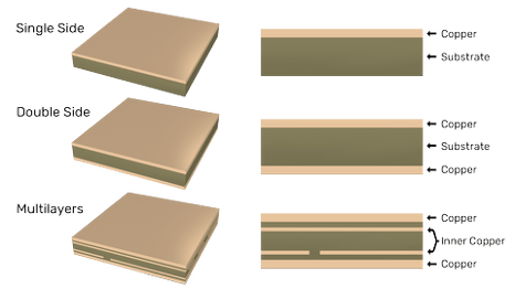
Typically, a low-layer-count board refers to PCBs with two to four layers. These boards are common for simpler electronics applications, prototypes, or in cases where budget and form factor limitations drive the design decisions. In these scenarios, our challenge is to ensure reliable power distribution without the flexibility that higher-layer-count boards naturally provide.
Let's review the design challenges we may be running into:
Power Distribution Challenges
Power distribution with fewer layers is tricky because it's not just a technical hurdle, it's a significant challenge. Simply put, fewer layers mean less room to neatly route power and ground traces, resulting in potential electromagnetic interference (EMI), voltage drops, and power integrity issues. If you've ever faced a design that required carefully balanced impedance or sensitive analog signals, you understand how critical managing your power distribution is.
Power Integrity
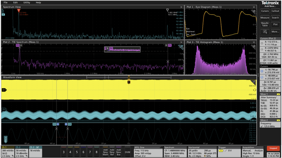
Image Credit: Tektronix - Analyzing Power Integrity[1]
One of the first terms you'll need to be comfortable with is "power integrity." Power integrity (PI) ensures that your design maintains a stable, noise-free power delivery system. Poor PI leads to voltage fluctuations, noise, and potential malfunction of sensitive components, especially microcontrollers, sensors, or RF devices. Managing PI effectively is even more critical on low-layer-count boards since space and routing options are limited.
Voltage Drop
Next, let's talk about "voltage drop." This happens when current travels through resistive elements of your PCB traces and components. On lower-layer PCBs, traces tend to be narrower and longer, increasing resistance and causing more significant voltage drops. That means your carefully chosen 3.3V or 5V rails could dip below the necessary levels for your components, potentially leading to erratic or degraded performance.
Ground Bounce
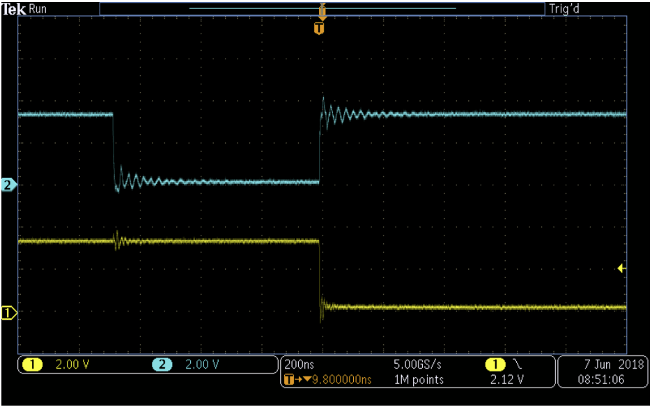
Image Credit: All About Circuits - How to Reduce Ground Bounce[2]
Another challenge I frequently encounter, and you likely have, is "ground bounce". Ground bounce occurs when return currents passing through ground traces cause fluctuations in the ground reference voltage. With fewer layers, return paths become convoluted and lengthy, increasing the risk of interference. This can wreak havoc, particularly in mixed-signal designs or circuits with high switching currents.
Power Distribution Tactics
Given the challenges posed by low-layer-count PCBs, it becomes imperative to employ strategic solutions to mitigate these issues effectively. Let's walk through some practical solutions you can consider when designing a low-layer-count PCB:
Strategic Use of Copper Pours
One effective way I've consistently handled power distribution challenges is by using strategic copper pours . Copper pours provide wider conductive paths for power and ground, and help in heat dissipation. For instance, by dedicating substantial copper areas on both sides of a two-layer PCB to power and ground, we significantly lower the resistance of these paths. This strategy reduces voltage drop and stabilizes ground reference levels, helping maintain the integrity of sensitive signals.
Wider Traces for Power
Always ensure that your power traces are sufficiently broad to handle expected current loads. A common mistake I've seen, especially in space-constrained designs, is using overly thin traces for power distribution. This approach might save space initially but can lead to reliability issues. Calculate trace widths based on anticipated current, ensuring you're well within safe operating limits to maintain voltage stability.
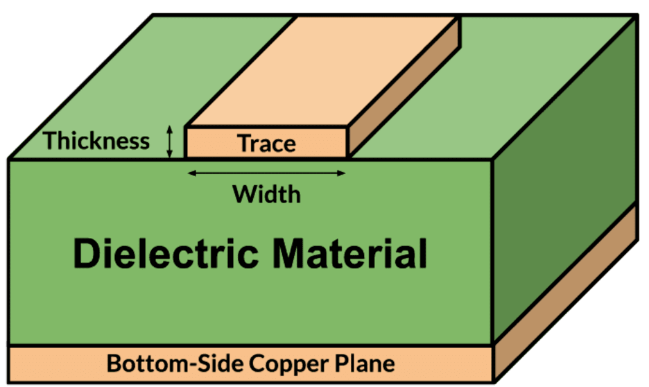
Image Credit: Cadence - Optimizing for PCB Trace Thickness vs Current Capacity
In one project, a compact IoT sensor board was designed with 10 mil (0.25 mm) wide traces carrying up to 2 amps of current to a Wi-Fi module. Although the board initially worked during lab testing, over time, the traces overheated during real-world use, causing intermittent resets and even delamination of the PCB layers. After investigation, the design was corrected by widening the power traces to 40 mils (1 mm), which solved the instability issues and significantly improved the device's reliability.
Optimal Component Placement
Strategic placement of components is crucial on low-layer-count PCBs. Power-hungry components, like regulators and microcontrollers, should be located close to their associated decoupling capacitors and power inputs. I've found that minimizing trace lengths between critical components reduces resistance and inductance, helping maintain stable voltage levels and significantly reducing noise.
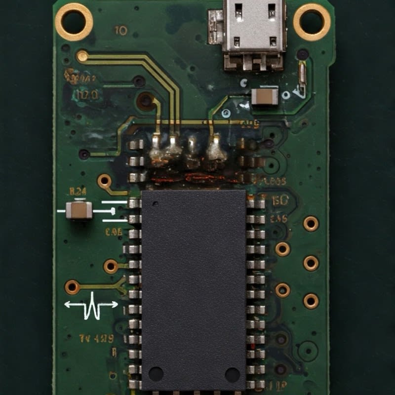
Via Stitching
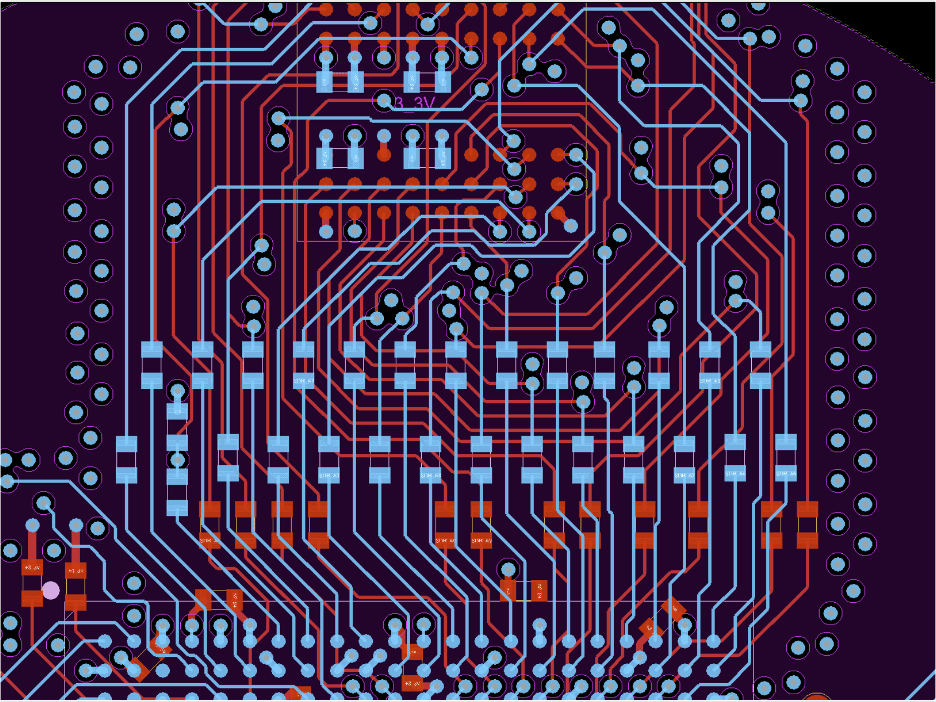
Image Credit: John Burkhert - The Case for Stitching Vias on Your PCB
Consider via stitching in situations where you might be using a four-layer PCB (with inner power/ground layers). We significantly enhance the board's thermal and electrical performance by strategically placing vias that connect different layers of ground or power planes. Via stitching helps lower the impedance of power paths, ensuring a cleaner and more stable power supply.
Design Examples
Now, let's talk briefly about specific scenarios where designing low-layer-count PCBs with optimized power distribution is necessary:
IoT Sensor Nodes
IoT devices are often small, battery-powered, and cost-sensitive. We rarely have the luxury of high-layer-count boards. By using wide traces, ground copper pours, and strategic capacitor placements, we can achieve stable power delivery without compromising the form factor or battery life.
Budget-Conscious Consumer Electronics
If you've ever designed consumer electronics intended for mass-market production, you know budget constraints are stringent. In these projects, every additional PCB layer can drastically impact production costs. Leveraging innovative power distribution strategies allows us to stick to lower-layer counts without sacrificing product reliability.
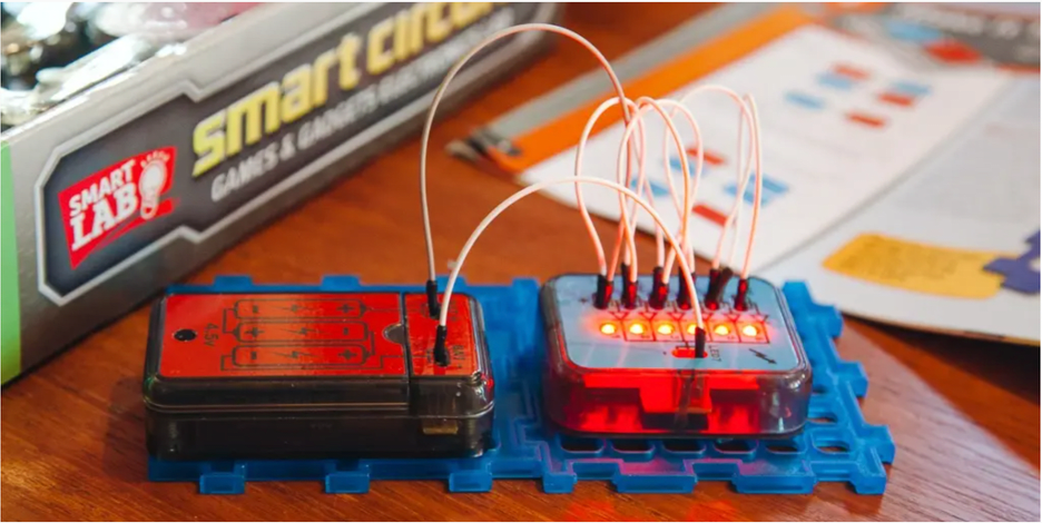
Rapid Prototyping and Educational KitsImage Credit: NY Times - The Best Electronics Kits for Kids and Beginners
Low-layer-count PCBs are also perfect for rapid prototyping and educational purposes, where simplicity and affordability are paramount. By effectively handling power distribution basics in these designs, we ensure learners and prototypers face fewer unforeseen technical hurdles, enabling a smoother learning curve and faster iteration cycles.
Key Takeaways
In this blog, we explored the challenges of power distribution on low-layer count circuit boards, such as voltage drops, ground bounce, and limited routing options. By employing strategic solutions like copper pours, wider traces, optimized component placement, and stitching, you create reliable and sustainable PCB designs that make the most of our available space and resources.
The best practice always involves combining good theoretical knowledge with practical experience. So, the next time you face a low-layer-count design challenge, don't hesitate to try these strategies. I'm confident you'll notice a significant improvement in the robustness and performance of your circuits.