PDN Design Guidelines Guide
Key Takeaways
-
A well-designed PDN preserves return paths and supports signal integrity in high-speed designs.
-
Split planes and impedance control require careful planning to avoid blocking return currents and maintain signal fidelity.
-
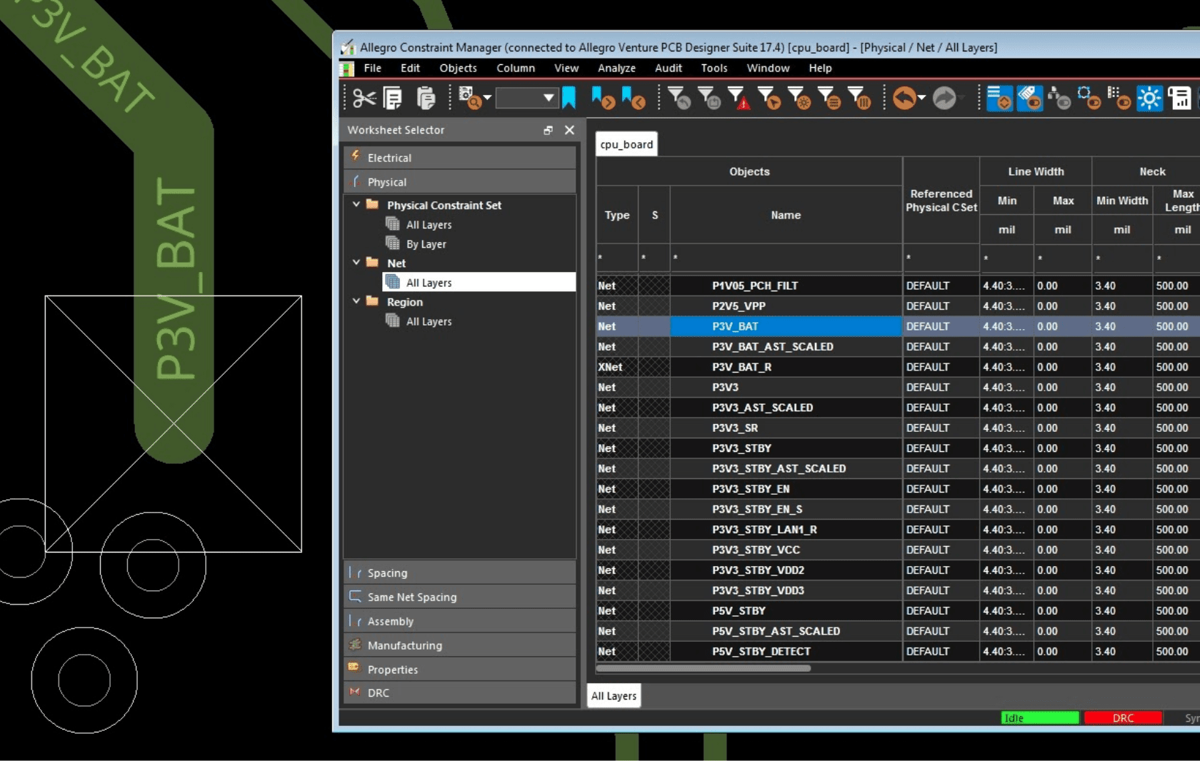
Allegro X simplifies PDN design through constraint management, real-time DRC, and power integrity visualization.

Every electronics engineer dreads an overloaded power strip sparking—a stark warning of what a stressed power distribution network (PDN) can cause. Though less dramatic, a poor PCB PDN can lead to failures and signal integrity problems. This guide outlines essential PDN design guidelines and demonstrates how the features within Allegro X can help you create robust and reliable power delivery systems for your circuit boards.
The Necessity of a Good Power Delivery Network on Your PCB
All active components on a PCB require clean, stable power. As device complexity, density, and operating speeds increase, the demands on the PDN have grown exponentially. A poorly designed PDN can manifest in several ways:
-
Excessive IR Drop: Voltage drops across power plane resistance can prevent components from receiving adequate voltage, especially under high current loads. Proper power plane sizing and placement of bulk decoupling help mitigate this.
-
Transient Load Instability: Sudden current demands (e.g., from fast clock edges or simultaneous switching events) can cause voltage dips or overshoots. Without sufficient low and high-frequency decoupling, these transients can destabilize power rails and cause functional errors.
-
Unexpected Resonance and Anti-Resonance: Improper decoupling capacitor selection and placement can lead to resonant peaks in the PDN impedance profile. These resonances can amplify noise or cause voltage instability at specific frequencies. Anti-resonance, often caused by mixing different capacitor values without careful layout, can introduce sharp impedance spikes that compromise power integrity.
-
Electromagnetic Interference (EMI): Fast-switching circuitry can become a source or victim of EMI. Power and ground planes act as shielding and current return paths, reducing radiated and conducted emissions when properly configured.
-
Ground Bounce (Simultaneous Switching Noise - SSN): High-speed digital systems often switch multiple signals simultaneously, inducing voltage noise in the ground reference. A low-impedance PDN with tight return paths helps suppress this and maintain signal integrity.
-
Power Ripples & Noise: Switching regulators and noisy digital blocks can inject ripples onto the power rails. These disturbances may couple into analog paths or sensitive logic, degrading performance. Proper decoupling, filtering, and layout practices are essential for noise suppression.
High-Density Power and Ground Connections
With the increasing switching speeds of modern digital circuits, the number of power and ground connections per integrated circuit (IC) has grown significant;y. Large processor devices, in ball grid array (BGA) packages, often include hundreds of power and ground pins, spanning multiple voltage domains and reference levels. These pins can draw substantial current , and ensuring stable, noise-free power delivery - free from voltage spikes, ripple, and high-frequency noise - requires a well engineered PDN. Beyond supplying clean power, the PDN also plays several critical roles, including controlling impedance across a broad frequency range, minimizing simultaneous switching noise (SSN), and supporting signal integrity through low-impedance return paths.
Power Delivery Network Design Common Challenges and Solutions
|
Design Guidelines |
Common Design Challenge(s) |
Design Guidelines Solutions |
|
Dense via fields (for power, ground, and signals on high-density parts) can perforate planes, creating obstacles that force return currents to take longer, more inductive paths, degrading signal integrity. |
|
|
|
Balancing the plane configuration to meet both power delivery needs (sufficient copper, low impedance) and the precise geometric requirements for controlled impedance routing across various signal layers. |
|
|
|
Creating "split planes" (partitioning a single copper layer to carry multiple voltages/grounds) is efficient for distribution but introduces additional discontinuities. These splits can block signal return paths if traces are routed across them. |
|
PDN Design Guidelines for Manufacturability
A PDN design may call for a non-symmetrical layer stackup, but PDN design guidelines dictate that symmetrical stackups are preferred, where top and bottom layers mirror each other. This preference stems from fabrication concerns—uneven stackups are more prone to warpage under high temperature and pressure, especially in larger boards. Warping can stress thin metal traces and solder joints, compromising signal integrity and mechanical reliability. To avoid these problems, circuit board designers should consider the following:
-
Keep the power and ground plane layers symmetrical in the board layer stackup, if possible, without compromising signal integrity.
-
Make sure that the prepreg and core layers are also symmetrical in their thickness throughout the board layer stackup.
-
Try to keep the densest copper layers of the board in the center of the stackup. Again, this must be done in conjunction with good signal integrity practices.
-
Use the same copper weight for the different plane layers.
-
Consider adding metal fills (copper pours) in areas of the board that don’t already have much metal on them.
-
Most importantly, check with your PCB manufacturer on your proposed board layer stackup before you commit to it in order to ensure that they will be able to fabricate it.
Thermal Management for Large Copper Areas
When designing a PDN with large copper areas - such as wide power planes or heavy copper pours - thermal management becomes a critical consideration to ensure reliability and prevent localized overheating. Large copper regions can effectively dissipate heat due to their high thermal conductivity, but they can also create thermal gradients if not properly balanced. To manage this, designers should ensure even copper distribution across the board to avoid hotspots and warping due to reflow. It’s important to maintain adequate copper thickness (e.g., 2 oz or more for high current paths) while avoiding isolated thermally conductive areas that lack sufficient vias for heat spreading to internal layers or heatsinks. Thermal vias placed under high power components or near VRM outputs should connect to internal planes to enable vertical heat dissipation. Additionally, designers should evaluate the temperature rise in power planes under expected current loads using thermal simulation tools, like Cadence Celsius, and ensure compliance with IPC-2152 current carrying capacity guidelines to avoid long term thermal stress on the board materials and components.
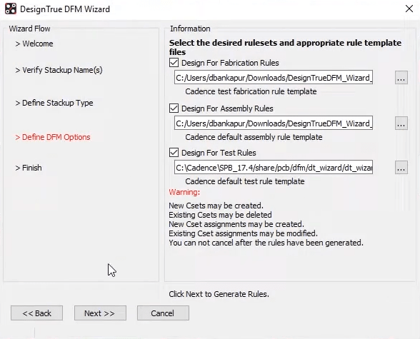
The DesignTrue DFM Wizard in Allegro X allows designers to set up fabrication, assembly, and testing checks from the beginning.
Leveraging Allegro X for Adherence to PDN Design Guidelines
Cadence tools offer several features to support PDN design guideline adherence throughout the layout process. Notably, Allegro X includes in design IR drop analysis, which provides real-time visibility into power integrity issues. It highlights pins with insufficient voltage on power nets, allowing immediate layout adjustments to ensure a reliable PDN. You can find out more information on how to create an effective PDN by looking at this E-book.
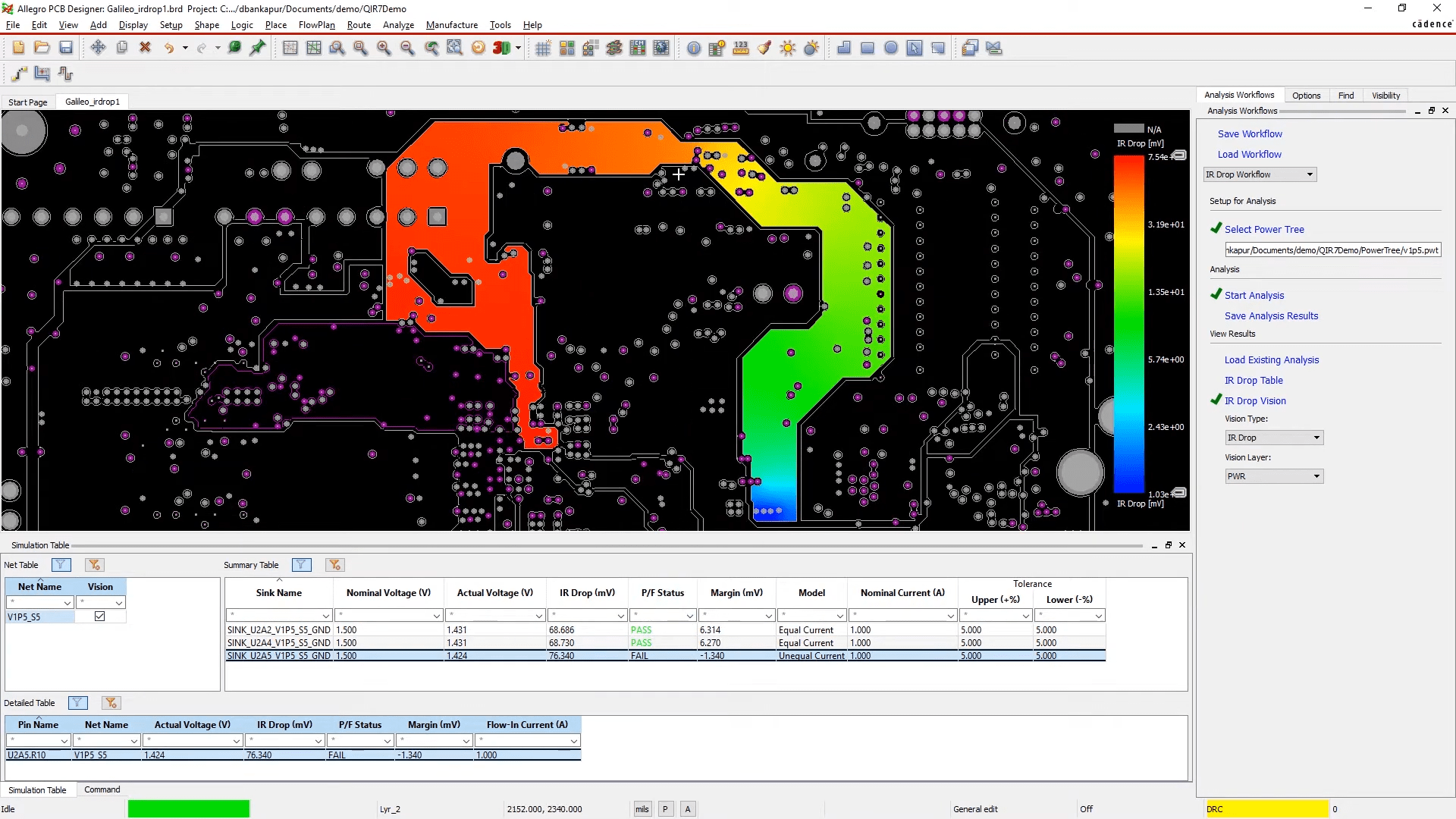
Tools such as the IR Drop Vision in Allegro X can help plan out an effective PDN.
Allegro X Features for PDN Design Guideline Adherence
|
PDN Design Need |
Challenge Addressed |
Allegro X Feature |
How It Helps |
|
Controlled Impedance and Return Path Routing |
Maintaining proper trace width, spacing, and return path continuity |
Enforces rules for trace geometry, spacing, and reference layers for various power net classifications. |
|
|
Split Planes and Multi-Net Planes |
Preventing blocked return paths and signal integrity loss due to plane splits |
Flags violations where signal traces cross split planes or violate power/ground constraints. |
|
|
High Current Via Design |
Vias undersized for high current cause voltage drop and thermal issues |
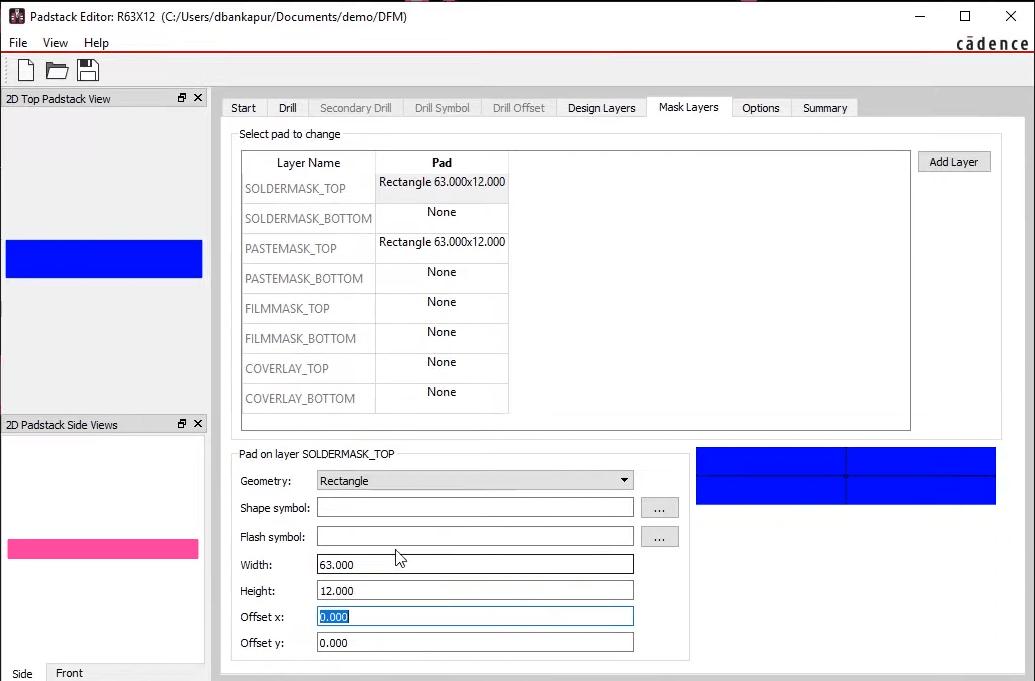
Allows custom via and pad design for current-carrying capacity, including multiple drill types and copper weights. |
|
|
Stackup Planning for PDN and Fabrication |
Unbalanced stackups cause warping and thermal stress |
Enables precise layer planning with symmetrical power/ground planes and dielectric balancing. |
|
|
Thermal Relief and Plane Connectivity |
Solid copper connections complicate soldering and thermal balance |
Sets thermal relief rules and manufacturability checks early in the design process. |
|
|
Power Integrity Analysis (IR Drop, Voltage Loss) |
Late detection of voltage drops can cause time-consuming rework |
IR Drop Analysis |
Provides real-time visualization of voltage distribution across power nets. |
|
Comprehensive PDN Simulation |
Complex PDNs require in-depth analysis beyond visual checks |
Sigrity X Integration, Impedance Analysis |
Enables AC/DC power integrity simulations, decap analysis, and impedance modeling. |
Power delivery network (PDN) design is critical for ensuring stable voltage, clean signal returns, and robust EMI protection in today’s dense, high-speed PCBs. With the Cadence Allegro X platform, designers can confidently tackle the challenges of adherence to PDN design guidelines. Explore Cadence PCB Design and Analysis tools for smarter, faster PCB design.
Leading electronics providers rely on Cadence products to optimize power, space, and energy needs for a wide variety of market applications. To learn more about our innovative solutions, subscribe to our newsletter or our YouTube channel.