Allegro X Advanced Package Designer Datasheet
Efficiently design complex packages with first-pass success
Market demand for more functionality is driving the move to advanced packaging to accommodate complex designs. To efficiently design these complex packages requires a sophisticated implementation tool that addresses both electrical and physical constraints. Cadence IC package design technology is recognized worldwide for its efficient, flexible, and reliable implementation of dense, advanced package designs. Integrated signal and power integrity analysis ensures that electrical and physical challenges can be jointly addressed throughout the design cycle. Using Cadence IC package design technology, designers can meet compressed schedule demands with first-pass success.
Cadence IC Package Design Technology
IC packaging is now a critical link in the silicon-package-board design flow. The Cadence Allegro platform offers complete and scalable technology for the design and implementation of PCBs and complex packages. Cadence IC package design technology allows designers to optimize complex, single- and multi-die wire bond and flip-chip designs for cost and performance while meeting short project timelines.
This constraint-driven, industry-standard technology enables system planning, advanced OSAT, and foundry-based package design, from single-die to complex systems. Cadence IC package design technology enables efficient wire-bond design techniques, constraint-aware substrate interconnect design, and detailed interconnect extraction, modeling, and signal integrity/power delivery analysis.
 Figure 1: Constraint-driven interactive wire bonding includes push-shove across multiple wire tiers, the 3D wire profile viewer/editor allows for multiple wire profiles to be created and supported, and referenced profile libraries enable manufacturing-aware design and accurate simulation
Cadence IC package layout design technology is available in several different products and tiers, including:
- Allegro X Advanced Package Designer (with license)
- Allegro X Advanced Package Designer SiP Layout Option (with license)
- Integrity System Planner (with license)
- Allegro X Advanced Package Designer Silicon Layout Option (with license)
- Allegro X Advanced Package Designer RF Layout Option (with license)
- Allegro PCB Symphony Team Design Option (with license)
- System Connectivity Manager (with license)
Benefits
- Technology file use-model simplifies and automates design setup
- Front-to-back schematic and schematic-less flows provide the industry’s most flexible model for connectivity management
- On-the-fly library generation streamlines data input
- Intelligent definitions of wire-bond, flip-chip, stacked, and embedded die configurations assure correct-byconstruction layouts
- Advanced bond-shell generation automates even the most complex multi-die, stacked wire-bonded layout
- Radial, all-angle push-and-shove routing addresses the unique routing challenges of BGA/LGA substrate layout
- BGA/LGA-specific DRC/DFM/DFA checks to guarantee a design that can be built correctly the first time
- 3D visualization and DRC checking for validating your design more accurately than a 2D solution
- Integrated flows with Cadence Innovus and Virtuoso IC design tools to streamline the co-design of ICs and packages
- Tight integration with Cadence Sigrity, Clarity, and Celsius solvers for fast and accurate electrical and thermal package validation
- Symphony Team Design Option enables multi-user concurrent editing of substrate layouts, reducing overall design time
- Silicon Layout Option extends Allegro X Advanced Package Designer capabilities to handle layout and mask-level verification of silicon substrates
- Used by over 400 customers worldwide
Layout Features
Constraint-Driven Physical Layout
Allegro X Advanced Package Designer includes all the functionality and features needed to design today’s advanced packages. Full online design rule checking (DRC) supports the complex, unique requirements of all combinations of laminate, ceramic, and silicon-based substrate technologies.
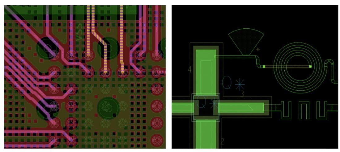 Figure 2: Additional capabilities for silicon-based technologies and RF packaging are available through the Silicon Layout Option and RF Layout Option
 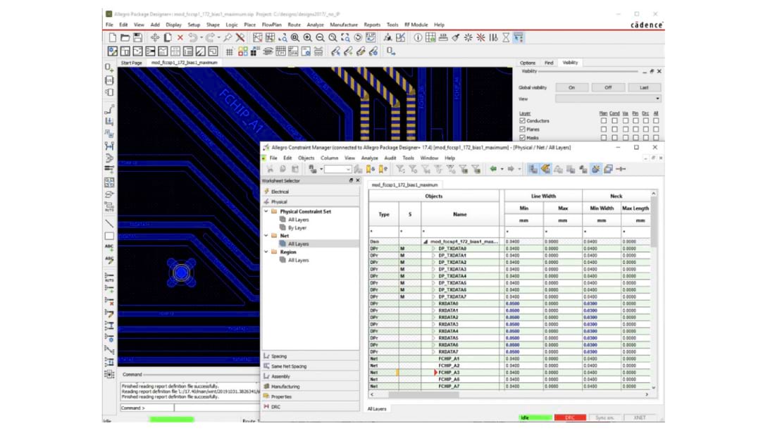 Figure 3: Comprehensive substrate physical virtual prototyping allows the engineer to evaluate the effects of physical design changes to signal integrity and signal performance
Multiple cavities, complex shapes, and interactive and automatic wire bonding are all supported. The easy-to-use Flow Manager walks you through each task and automates the process of creating the building blocks of an IC package, including the import and creation of die, package, routing, plating bars, and etchback. Single and multiple die, die stacks, and two-sided die are supported; die and substrate wizards automate definition of these library elements with your choice of ASCII standard formats (Die Text, DEF, AIF), die abstracts, or a form-driven user interface, such as ”text in” wizards.
 Figure 4: Complex stack-die construction, including spacers and interposers, is managed by the Die Stack Editor, connectivity is supported on both sides of the die
Sophisticated Substrate Modeling and Rule Checking
Design accuracy can be verified against a complete set of physical and electrical design rules (constraints). Physical constraints are physical design guidelines, established in a user-defined technology file, that ensure manufacturability. Electrical constraints are signal delay, timing, and distortion specifications for critical nets. Allegro PCB DesignTrue DFM Technology’s checks ensure designs meet manufacturers’ requirements. Designs can be dynamically checked against these constraints throughout the design process to ensure they are meeting manufacturing and electrical specifications. Immediate feedback is provided by DRC markers as well as flagging violations in the spreadsheet-based Constraint Manager.
Process Technology Reuse
Both substrate stack-up and constraint information are captured in a technology file, which can then be reused for other designs of similar structure to further reduce cycle time on future designs, either in portions or for the entire design. Substrate suppliers can provide tech files that contain critical design rules to help drive a correct design methodology. Manufacturers can overlay their assembly and manufacturing requirements over the top of design constraints. Multiple tech files can be used from different suppliers to ensure manufacturability at secondary suppliers.
Wirebond, Flip-Chip, and Copper Pillar Escape Patterns
As wire bond attach is still the most popular packaging method, Allegro X Advanced Package Designer is designed to provide fast, powerful, and flexible bondshell creation and editing. Ground-up, constraint-driven, automatic bondfinger array placement can be used with multiple stacked die, staggered die pads, multiple bond levels, multiple bondrings, and both symmetrical and non-symmetrical designs. Unique push-and-shove bondfinger editing enables extremely complex bondshells to be developed in minutes, delivering unparalleled capability and productivity. True wire profile support enables DFM-driven design using manufacturing-verified wire loop data. Loop profile libraries ensure that wire bond patterns meet manufacturing signoff. This is supported by extensive wirebond rules and constraints that provide real-time design feedback. Powerful metal-shape editing tools allow rings to be customized, split, and assigned to multiple voltages with just a few mouse clicks. Interactive substrate routing and wire bond connections work intelligently through pad entry rules, any-angle pad exit routing, and wire bond finger stubs that stay aligned to bondfingers when the fingers are moved.
For bump and pillar-attach, a proven set of tools assists the user in creating and replicating the complex routing escape patterns found in today’s high-density designs. Both automatic and semi-automatic tools are included. Once the patterns are created, the designer can quickly propagate them around the die.
Automatic Bump-to-Package Pin Assignment and Route Feasibility
Schematic and netlist-based design methodologies are supported, leveraging the Integrity System Planner for upfront system planning, and standalone netlist or sophisticated netlist management leveraging a unique System Connectivity Manager that forms part of the SiP Digital Architect product. Logic assignments can be created on the fly, or assignment algorithms can determine the best routable assignments based on existing design rules. Nets are assigned by layers based on net constraints and route channel availability. Differential pair-defined bumps are automatically assigned to adjacent package pins accord- ingly. A net-per-layer assignment visualization tool also allows designers to visualize the completed assignment. Additional route planning can be done for high-speed and interface buses with flow designer technology that bundles net groups together and allows route plans to be visualized, focused on the ordering and assignments at the ends of the buses.
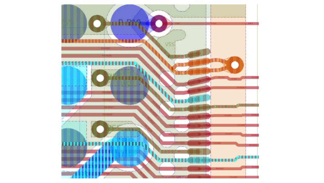 Figure 5: Constraint-driven interactive, auto-interactive, and full auto-routing tools are included that support orthogonal, 45s, and any-angle routing
Interactive, Auto-Interactive, and Automatic Routing
Allegro X Advanced Package Designer and the SiP Layout Option integrate a suite of tools for interactive and automatic rules-based routing capabilities. The result is fast and accurate routing of any type of IC package design— whether an all-angle, single-layer, wirebonded design or a silicon interposer on a multi-layer build-up substrate—with both interactive and automatic routing technology to quickly create manufacturing-quality interconnect (see Figure 5).
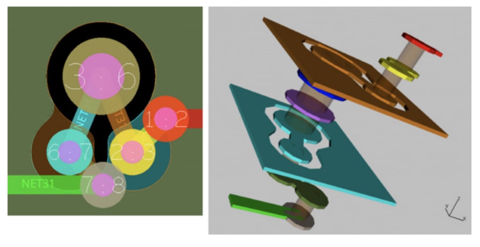 Figure 6: Constraint-driven HDI design allows designers to rapidly implement and update repetitive complex via structures, including return path vias, for escape and layer transitions
HDI Design
High-density interconnect (HDI) / build-up layer technology is pervasive in almost all IC package design using routable organic substrates and fine-pitch flip-chip devices. Allegro X Advanced Package Designer has comprehensive constraint-driven HDI design capabilities linked to automation-assisted interactive design. Comprehensive micro-via class rules linked to editing capabilities enable the designer to meet manufacturing requirements and achieve desired design and productivity goals (see Figure 6).
Team Design: Design Partitioning and Symphony Concurrent Design Option
Cadence provides multi-user, concurrent design methodologies for faster time to market and a reduction in layout time. Design partitioning allows multiple designers to work concurrently on a layout by distributing portions of the design to multiple users. Designers can partition designs into multiple sections or areas for layout and editing by several design team members. The partitioning can be vertical (“cake slice”) or horizontal (layer-based). As a result, each designer can view all partitioned sections and update the design view for monitoring the status and progress of other users sections. This can dramatically reduce overall design cycles and accelerate the design process.
The concurrent engineering option, Allegro PCB Symphony Team Design Option, shortens the largest portion of the package layout design cycle. Its shared canvas provides a low-overhead environment that enables multiple designers to work on the same design, on the same canvas, and at the same time without the set-up requirements of a partitioned project. The more routing engineers you add, the faster your team can finish routing. While in the concurrent team design environment, designers can use features of Allegro X Advanced Package Designer and the SiP Layout Option to accelerate design completion: shape editing and shape design for power delivery, interactive etch-editing commands and Allegro auto-interactive phase tune (AiPT) and auto-interactive delay tune (AiDT) capabilities, as well as dynamic shape voiding during routing, to name a few.
DesignTrue DFM and ARC
(Core Rules included, all rules available with the SIP Layout Option license)
The comprehensive design for manufacturing (DFM) checker and assembly rule checker (ARC) provide hundreds of checks to address the requirements of your manufacturer. Checks can be executed as a check-group, individually, or as a custom selection. Check results appear in the violation browser and as graphical markers in the design.
Extensive Manufacturing Output Capabilities
All types of data likely to be required can be generated from documentation to tooling. Users can easily create bond diagrams, dimension documents, format drawings, and various output files containing critical package manufacturing data. With the SIP Layout Option, design variants can be created for bond and stacking options, as well as assessing process variance on DRC and signal integrity. Manufacturing output supports Gerber, IPC2581, DXF, AIF, and GDSII.
Most package OSATs and foundries currently use Cadence IC package design technology. This pervasiveness allows users to send an Allegro design database directly to the foundry as manufacturing input, greatly compressing throughput times and eliminating inaccuracies. The foundry can use the database to enhance manufacturing yields and implement any last-minute changes to the package without inadvertently compromising the original specifications. (Contact your manufacturer to confirm their specific capabilities.)
PCB System-Level Handoff
Allegro X Advanced Package Designer not only bridges the gap between silicon and package design, but also links package and PCB design. All data required for PCB-level floorplanning and layout is automatically generated—physical footprint, schematic symbol, and device models. Also included is a symbol (die or BGA) export that can be read in spreadsheet tools. These capabilities compress set-up time and increase data accuracy for systems designers.
Package Signal and Power Integrity Features
Detailed interconnect extraction, 3D package modeling, and power-aware signal integrity and thermal analysis are available with Cadence Sigrity, Clarity, and Celsius technologies. These capabilities enable a package analysis and modeling solution that begins with early performance assessment and DC and AC PDN analysis, and moves to full-package extraction with hybrid solvers or detailed extraction of package segments with 3D full-wave solvers. The following technologies are available:
- A package assessment engine that allows quick detection of problematic package design practices, including detection of excessive inductive package pins, uncontrolled impedances, and high coupling
- A power-aware hybrid solver extraction engine, enabling RLGC and S-parameter model extraction of the complete coupled signal and PDN
- A full-wave 3D solver for high-frequency interconnect extraction of detailed structures within IC packages
- IR drop analysis, including electricalthermal co-simulation that considers both component and Joule heating, space-dependent temperature distribution, and current density computation for planes, vias, and interconnects
IC package performance assessment can begin at early stages of physical design, long before final package layout. Feasibility studies can be performed with initial connectivity to help determine which package type provides the best electrical performance for the lowest cost. For example, DC IR drop and current constraint-driven stack-up options, as well as signaling topology tradeoffs, may be explored and decided. As the package design continues, signal and PDN models can be extracted for comparison against RLC parasitic constraints and signals characterized for key attributes such as impedance and crosstalk or insertion and return losses. Thermal considerations may also be explored through the available coupled electro-thermal analysis capability. As the design reaches its final stages, full package assessment (including IR drop) and model extraction can be performed and an HTML signoff report generated to ensure that any significant problems are caught and the design fully documented. For packages expected to operate at high frequency, 3D full-wave extraction can be performed on critical package regions to ensure package performance specifications are met.
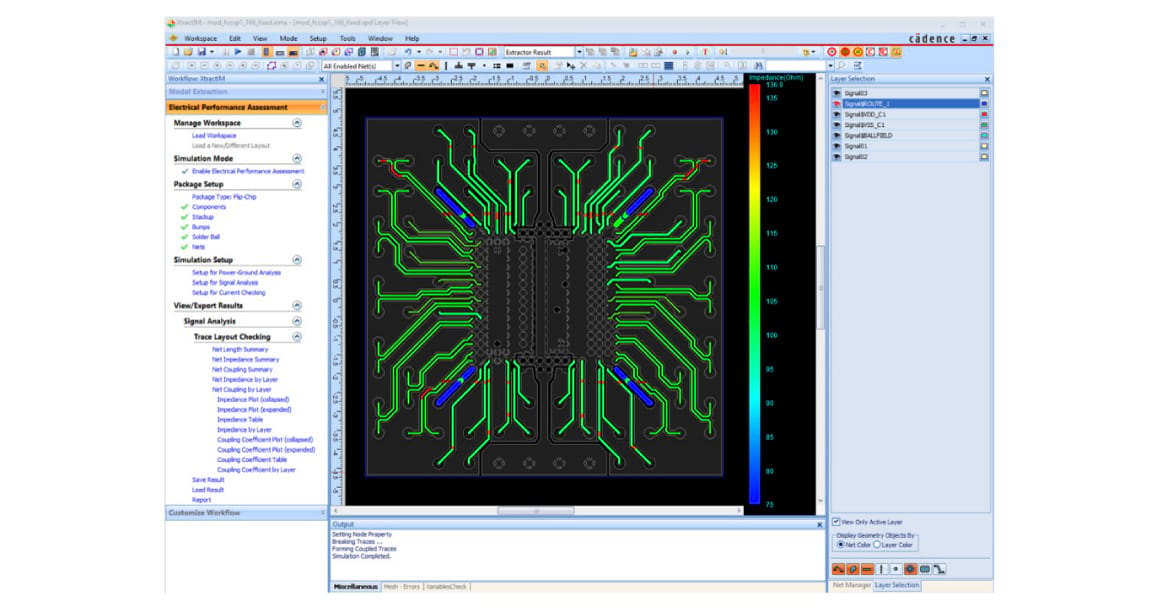 Figure 7: Sigrity extraction and 3D modeling technology is directly integrated, enabling comprehensive rapid analysis and simulation model creation
3D Design Viewer Features
The Cadence 3D Design Viewer is a full, solid model 3D viewer and 3D wirebond DRC solution for complex IC package designs and included with Allegro X Advanced Package Designer. It allows users to visualize and investigate an entire design, or a selected design subset, such as multiple wirebond tiers with multiple wire bond profiles. It provides a common reference point for cross-team design reviews.
Intelligent 3D Design Viewing
While a 2D representation is ideal for substrate layout, interconnect planning, and metal fill creation, this view does not lend itself well to the design, management, or verification of complex die stacks and 3D integration. The design complexity and density involved require a more realistic approach. The Cadence 3D Design Viewer meets this need by providing an IC package designer with the ability to physically visualize a design as it will actually look during manufacture. A designer can interactively zoom, pan, and rotate the 3D view as well as select from a set of pre-defined views.
Interactive Markup
During 3D design viewing, an engineer can create “markup” jpeg snapshots for design reviews and/or design documentation that include the ability to add basic shapes, arrows, and text. This is especially useful for communications with design chain partners and test and assembly manufacturing departments.
3D Wirebond Clearance Design Rule Checking
Rules are defined and stored as part of the Allegro X Advanced Package Designer design session. Completely user defined, these rules can be used to check 3D clearances between wires and components in the design.
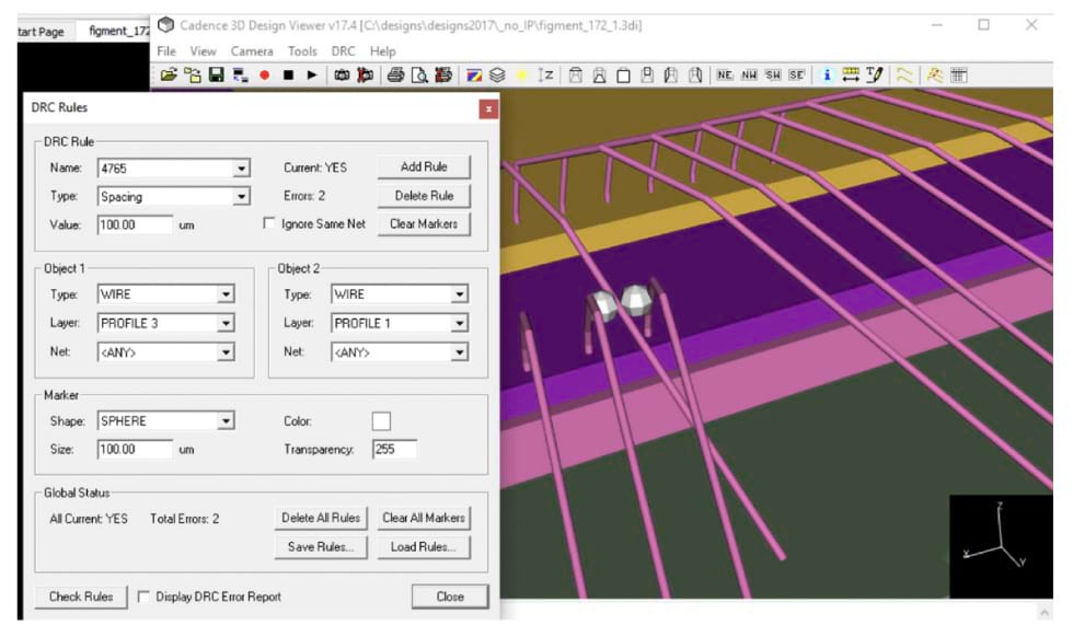 Figure 8: 3D interference rules (wire to wire and wire to object) are available through the 3D Viewer (included), using accurate wire curvature models
Operating System Support
- Linux
- Windows
Cadence Services and Support
- Cadence application engineers can answer your technical questions by telephone, email, or internet—they can also provide technical assistance and custom training.
- Cadence-certified instructors teach more than 70 courses and bring their real-world experience into the classroom.
- More than 25 Internet Learning Series (iLS) online courses allow you the flexibility of training at your own computer via the internet.
- Cadence Online Support gives you 24x7 online access to a knowledgebase of the latest solutions, technical documentation, software downloads, and more.
- For more information, please visit support and training .