PCB Manufacturing Checklist for Flawless DFM
Key Takeaways
-
Implement actionable PCB manufacturing checklist steps from schematic through post-fab.
-
Collaborate closely with your contract manufacturer—verify exported manufacturing data (Gerbers, drill files, netlists) in CAM tools to catch errors before production.
-
Automate critical DFM and DFA rule checks directly in OrCAD X.

Following a good PCB manufacturing checklist ensures your PCBs will come out with optimal reliability and function.
Every PCB design project must undergo a rigorous DFM-focused review to ensure manufacturing accuracy and high yield. These reviews aim to detect errors that could compromise manufacturability, assembly reliability, and compliance with fabrication standards.
When you’re ready to perform a review with your team or a client, one way to keep everyone on track is to use a PCB manufacturing checklist. PCB design reviews normally happen on the front end, before sending a design into a fabrication house. A post-build design review also occurs during product development, involving further inspections of the physical board and testing the board for functionality.
This guide covers essential DFM quality checks, actionable steps, and best practices to achieve flawless PCB manufacturing.
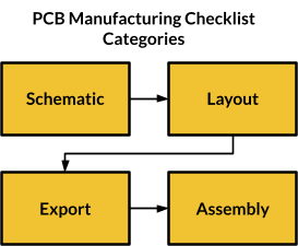
A PCB manufacturing checklist should cover the full PCB design process of schematic, layout, export, and assembly.
What Goes Into PCB Inspection
Focus your DFM checklist on key phases:
-
DFM review of schematic data and component footprints
-
DFM review of PCB layout and layer stackup
-
Verification of manufacturing data exports (Gerber/ODB++/IPC-2581)
-
After assembly, the design should also be tested and qualified against your performance standards to ensure the device will work as intended.
The PCB Manufacturing checklist can be in any document format, (e.g. Word document, spreadsheet, or a shared resource). Once the project is shared with the PCB design reviewer, a fresh checklist can also be generated and shared with the reviewer.
For the first phase, verify all footprints and library data conform to fabrication house guidelines:
1. Actionable Schematic and Footprint DFM Checks
|
Step |
Actions |
|
Export Fab Guidelines & Library Comparison |
- Obtain your fab house’s latest footprint and pad-stack libraries. - Cross-reference every schematic symbol’s linked footprint against recommended IPC Class 2/3 dimensions. |
|
Pad Dimension Verification |
- Run a “pad check” report listing X- and Y-dimensions for all SMD and through-hole pads. - Flag any pad with < 0.25 mm annular ring or < 0.1 mm drill-to-pad clearance. |
|
Courtyard & Solder-Mask Expansion |
- Inspect each courtyard outline for ≥ 0.5 mm clearance to adjacent parts. - Verify solder-mask expansion settings match fab tolerances (e.g. +0.1 mm small pads). |
|
Thermal Relief & Copper Pour Clearances |
- Check thermal spokes on through-hole pads meet minimum spoke width (e.g.,≥ 0.2 mm). - Confirm copper pour clearance is ≥ 0.2 mm from GND pours around pads. |
|
Via Pad & Annular Ring Audit |
- Generate a via-drill report and confirm every via has ≥ 0.15 mm annular ring. - Spot-check ring dimensions by drill size in your footprint library. |
|
Plating & Metallization Requirements |
- Review spec for selective plating (ENIG vs. HASL) and tag footprints needing castellations/gold fingers. - Annotate special pads with “No-mask” and “Gold-plate” flags. |
Many of these aspects can be checked using the DRC engine in your PCB design software, but only as long as the constraints are correctly defined in the system.
Design Considerations:
-
Component Density: Balance pad-pitch vs. assembly yield; avoid <0.4 mm pitch unless your assembler routinely runs micro-BGAs.
-
Thermal Management: For heat-sinking pads, include multiple thermal relief spokes or dedicated copper areas sized per IPC-2221A.
-
Testability: Add test-point pad options to footprints for critical nets or reserve net-tie pads if boundary-scan isn’t available.
Best Practices:
-
Library Governance: Lock down your approved footprint library with version control; require sign-off before new footprints are published.
-
DRC Automation: Automate pad and annular-ring checks in your pre-PCB-layout DRC rule set to catch out-of-spec dimensions immediately.
-
Fab Collaboration: Schedule a quarterly review with your contract manufacturer to update your DFM rules based on their yield and process changes.
2. PCB Layout and Stackup DFM Checks
In the PCB layout, layers need targeted DFM inspections:
|
Layer Category |
DFM Checks |
|
Signal Layers |
- Trace width/spacing meets fab requirement - Copper weight on each layer- Stackup symmetry - Trace-to-pour, pour-to-pour, pour-to-pad clearances - Drilled hole wall clearances - Vias/pads obey IPC Class 2/3 standards |
|
Plane/Pour Layers |
- Antipads around vias - Plane boundaries near board edge - Copper weight on each layer - Stackup symmetry - Check plane splits and stitching vias for power integrity |
|
Mask Layers |
- Solder mask openings (top & bottom) only expose intended pads - Check tenting rules do not block critical pads - Validate solder mask expansion matches misregistration tolerances |
|
Paste Mask Layers |
- Paste mask openings (top & bottom) align with solder mask - Eliminate merged paste openings - Adjust openings to prevent tombstoning or insufficient solder - Square openings for thermal pads |
|
Silkscreen Layers |
- Remove silkscreen from pads - Keep reference designators within board outline - Add manufacturing identifiers (board revision, date code) |
|
Mechanical Layers |
- Check collisions between component bodies - Ensure mechanical layers match element outlines - Define mechanical layers for board cutouts, routed slots, plated elements - Expansion components have mechanical outlines - Assign 3D bodies where required |
PCB Manufacturing Checklist for Silkscreen
The silkscreen layer on the PCB layout should be examined as part of general circuit board cleanup and tidiness. Most often, the silkscreen layer will need to be organized after placement and routing are finished so that all important reference designators will be confined within the board shape boundaries. You can also take some time to hide any designators that do not need to appear in the production board.
There are other pieces of information that should be added to the silkscreen layer if they are not present already:
-
The most recent part number and revision
-
Company or producer logo
-
Lot number, serial number, etc. (usually added by the manufacturer)
-
FCC, CE, UL, ESD, and any other safety/compliance markings
-
Special legend markings indicating expansion board placement, cable placement, etc.
-
Will these be visible if the board is assembled into an enclosure or multiple-board system?
Verify these are present in the PCB layout in silkscreen layers during a review. Other problems like clearances between silkscreen elements will be caught by the DRC system in your design software.
Solder Mask Manufacturing Checklist
The solder mask layer shows openings in the solder mask on the surfaces of the board. The very first point to check is that openings are located on component pads for SMD parts and through-hole mounted parts. Sometimes, a tenting rule can cover these parts so that the pads are no longer visible, and this will block the application of solder paste, even if the paste mask layer is correct. Other things that must be applied in the solder mask layer are any openings in the solder mask required for plating copper, such as on large copper islands or RF circuits.
-
Does any tenting rule close SMD pads?
-
Are any plated areas visible through the solder mask opening?
-
Does the expansion around SMD pads create small solder mask slivers?
-
Does expansion around pads match misregistration tolerances?
Solder mask is often formed automatically by applying a solder mask expansion rule - this is exactly how tenting is applied. Below are some typical expansion values that should be checked. These could be applied in the footprint, but your PCB layout software might override these values, so this should be part of the inspection in the PCB.
-
SMD/through-hole pads: +0.025 mm (+1 mil) to +0.1 mm (+4 mil)
-
Vias (non-tented): +0.025 mm (+1 mil)
-
Board edge & plated features: 0 mm (0 mil)
Paste Mask PCB Manufacturing Checklist
The paste mask layer shows openings where solder paste is applied and should generally overlap with the solder mask layer. In the PCB editor, the two layers can be overlaid on each other so that the paste mask layer corresponding to solder mask openings can be identified. Paste mask openings have to be applied in the library data, but this can be overridden in the PCB layout data, so the checks should happen in the PCB layout for your project.
Paste mask layers are one area where DFA problems are hiding. In particular, paste mask layers define where solder paste will be applied, and the paste mask opening has to be sized so that the right amount of solder paste is placed onto the surface mount pads for assembly. Some problems to correct include:
-
If two SMT components are close enough to each other, an error may occur where the associated paste mask openings for each component merge into one. For this reason, make sure to check for merged paste mask openings between components; this should flag a DRC error
-
Reduce paste mask openings where necessary on SMD components to prevent floating
-
Paste mask openings on thermal pads should be divided into squares
3. Manufacturing Data Export Verification
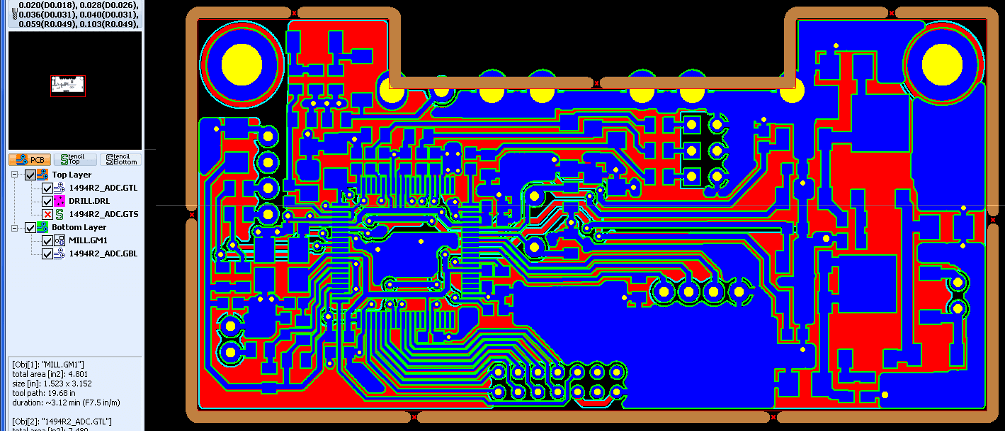
Initial manufacturing data inspections are in some ways quite simple. PCB design software allows for export of manufacturing data into standard formats (Gerbers, ODB++, or IPC-2581) that can then be used in CAM tools to view the production data.
Perform a layer-by-layer comparison in CAM software:
-
Gerber vs. CAD layers (copper, mask, silkscreen, mechanical)
-
Export and review drill files and toolmaps for correct drill sizes
-
Validate assembly drawings include polarity and component orientation
-
Load netlist into CAM tool to check for opens/shorts against copper
For assembly, the manufacturing data needs to be checked carefully against the following layers:
-
Paste mask top and bottom
-
Solder mask top and bottom
-
Drill table data
Manufacturing data (specifically layer data) also needs to be compared against a netlist for the PCB. When the netlist/wirelist export is loaded into a CAM tool with the Gerber data, this allows shorts and opens to be identified by looking at copper connections and comparing them against the netlist data. This is typically how fabricators will do an initial engineering review of the board, just to ensure that any design errors were not overlooked by the PCB designer.
4. Post-Fabrication Quality Checks
Inspect finished boards for compliance with fabrication tolerances. Tests come in progressively higher levels of complexity and precision, and you may need to implement some design for test practices to streamline your test procedures. Inspect finished boards for compliance with fabrication tolerances:
-
Visual inspection for etch undercut, solder mask registration, and board edge quality
-
Measure critical dimensions: board thickness, hole sizes, trace widths
-
Electrical continuity tests for key nets and ground/power integrity
-
Cross-section analysis for multilayer stackup integrity (optional)
More advanced tests for production boards will include environmental testing and more advanced stress testing, such as thermal cycle testing and power surge testing. Read this other article to learn more about stress tests in PCBAs.
Continuous Improvement of the DFM Checklist
Regularly review fabrication feedback and failure reports to update your DFM checklist. Add new checks for issues like solder bridging, insufficient annular rings, or warpage trends.
If there is some error or defect that is noticed repeatedly, consider adding that item to your PCB inspection checklist. As quality is continuously evaluated and new issues are identified, investigate these and try to determine the root cause. If a root cause can be determined, update your design process, quality controls, and inspection checklists to make sure these problems are not repeated.
So what should you do to ensure all identified errors are incorporated back into the PCB design data? Make another checklist! A simple checklist can be prepared based on test and inspection results following the table format below.
OrCAD X has built-in design for manufacturing capabilities, ensuring best adherence to your PCB manufacturing checklist.
PCB Manufacturing Checklist Adherence with OrCAD X
|
OrCAD X Feature |
How It Helps with Your DFM/DFA Checklist |
|
Constraint Manager |
|
|
Real-Time DFM Checks |
|
|
Interactive DRC Markers |
|
|
Panelization & Fiducial Support |
|
|
DFT/Test-Point Placement |
|
|
Manufacturing Export Verification |
|
|
Constraint-Driven Stackup Editor |
|
OrCAD X enables tight integration of DFM and DFA rules management to be directly mapped to each step of your PCB manufacturing checklist. By defining pad-stack and clearance constraints once in the Constraint Manager, you will ensure that schematic footprints, layout clearances, solder-mask expansions, and panel-level requirements are all automatically validated. This will save time and dramatically reduce the risk of late-stage fab or assembly failures.
By integrating your PCB manufacturing checklist directly into OrCAD X, you can automate DFM and DFA rule checks. This will ensure that pad dimensions, solder-mask expansions, via annular rings, panelization requirements, and more, are validated in real-time. Get started today: begin your OrCAD X Free Trial to experience constraint-driven design verification firsthand, or learn more about the full capabilities of the OrCAD X platform.
Leading electronics providers rely on Cadence products to optimize power, space, and energy needs for a wide variety of market applications. To learn more about our innovative solutions, subscribe to our newsletter or our YouTube channel.